SBOS968C june 2022 – july 2023 OPA186 , OPA2186 , OPA4186
PRODUCTION DATA
- 1
- 1 Features
- 2 Applications
- 3 Description
- 4 Revision History
- 5 Pin Configuration and Functions
- 6 Specifications
- 7 Detailed Description
- 8 Application and Implementation
- 9 Device and Documentation Support
- 10Mechanical, Packaging, and Orderable Information
Package Options
Mechanical Data (Package|Pins)
Thermal pad, mechanical data (Package|Pins)
- D|8
Orderable Information
3 Description
The OPA186, OPA2186, and OPA4186 (OPAx186) are low-power, 24-V, rail-to-rail input and output, zero-drift operational amplifiers (op amps). These op amps feature only 10 µV of offset voltage (maximum) and 0.04 µV/°C of offset voltage drift over temperature (maximum). These devices are a great choice for precision instrumentation, signal measurement, and active-filtering applications.
The low quiescent current consumption of 90 μA makes the OPAx186 an excellent option for power-sensitive applications, such as battery-powered instrumentation and portable systems.
Moreover, the high common-mode architecture along with low offset voltage allows for high-side current shunt monitoring at the positive rail. These devices also provide robust ESD protection during shipment, handling, and assembly.
| PART NUMBER | CHANNELS | PACKAGE(1) |
|---|---|---|
| OPA186 | Single | D (SOIC, 8) |
| DBV (SOT-23, 5) | ||
| OPA2186 | Dual | D (SOIC, 8) |
| DDF (SOT-23, 8) | ||
| OPA4186 | Quad | D (SOIC, 14) |
 High-Side Current Shunt Monitor Application
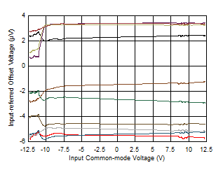
 VOS vs Input Common Mode
Voltage