SBOS850 December 2017 OPA192-Q1 , OPA2192-Q1
PRODUCTION DATA.
- 1 Features
- 2 Applications
- 3 Description
- 4 Revision History
- 5 Pin Configuration and Functions
-
6 Specifications
- 6.1 Absolute Maximum Ratings
- 6.2 ESD Ratings
- 6.3 Recommended Operating Conditions
- 6.4 Thermal Information: OPA192-Q1
- 6.5 Thermal Information: OPA2192-Q1
- 6.6 Electrical Characteristics: VS = ±4 V to ±18 V (VS = 8 V to 36 V)
- 6.7 Electrical Characteristics: VS = ±2.25 V to ±4 V (VS = 4.5 V to 8 V)
- 6.8 Typical Characteristics
- 6.9 Typical Characteristics
- 7 Parameter Measurement Information
- 8 Detailed Description
- 9 Application and Implementation
- 10Power-Supply Recommendations
- 11Layout
- 12Device and Documentation Support
- 13Mechanical, Packaging, and Orderable Information
Package Options
Mechanical Data (Package|Pins)
- DGK|8
Thermal pad, mechanical data (Package|Pins)
Orderable Information
1 Features
- Qualified for Automotive Applications
- AEC-Q100 Qualified with the Following Results:
- Device Temperature Grade 1: –40°C to +125°C Ambient Operating Temperature
- Device HBM ESD Classification Level 3A
- Device CDM ESD Classification Level 4A
- Low Offset Voltage: ±5 µV
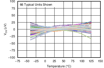
- Low Offset Voltage Drift: ±0.2 µV/°C
- Low Noise: 5.5 nV/√Hz at 1 kHz
- High Common-Mode Rejection: 140 dB
- Low Bias Current: ±5 pA
- Rail-to-Rail Input and Output
- Wide Bandwidth: 10 MHz GBW
- High Slew Rate: 20 V/µs
- Low Quiescent Current: 1 mA per Amplifier
- Wide Supply: ±2.25 V to ±18 V, 4.5 V to 36 V
- EMI/RFI Filtered Inputs
- Differential Input Voltage Range to Supply Rail
- High Capacitive-Load-Drive Capability: 1 nF
- Industry-Standard Package:
- Single and Dual Channel in VSSOP-8
2 Applications
- Motor Control for Automotive
- Traction Inverter
- On-Board Charger
- Precision Current Sensing
3 Description
The OPAx192-Q1 family (OPA192-Q1 and OPA2192-Q1) is a new generation of 36-V, e-trim operational amplifiers. The OPAx192-Q1 family of operational amplifiers use e-trim™, a method of package-level trim for offset and offset temperature drift implemented during the final steps of manufacturing after the plastic molding process. This method minimizes the influence of inherent input transistor mismatch, as well as errors induced during package molding.
These devices offer outstanding dc precision and ac performance, including rail-to-rail input/output, low offset (±5 µV, typical), low offset drift (±0.2 µV/°C, typical), and 10-MHz bandwidth.
Unique features such as differential input-voltage range to the supply rail, high output current (±65 mA), high capacitive-load drive of up to 1 nF, and high slew rate (20 V/µs) make the OPAx192-Q1 a robust, high-performance operational amplifier for high-voltage industrial applications.
The OPAx192-Q1 family of op amps is available in an 8-pin VSSOP package and is specified from –40°C to +125°C.
Device Information(1)
| PART NUMBER | PACKAGE | BODY SIZE (NOM) |
|---|---|---|
| OPA192-Q1 | VSSOP (8) | 3.00 mm × 3.00 mm |
| OPA2192-Q1 |
- For all available packages, see the package option addendum at the end of the data sheet.
OPAx192-Q1 Maintains Ultra-Low Input Offset Voltage Over Temperature
