SBOS962F April   2020  – March 2023 OPA205 , OPA2205 , OPA4205

PRODMIX  

  1. Features
  2. Applications
  3. Description
  4. Revision History
  5. Pin Configuration and Functions
  6. Specifications
    1. 6.1 Absolute Maximum Ratings
    2. 6.2 ESD Ratings
    3. 6.3 Recommended Operating Conditions
    4. 6.4 Thermal Information: OPA205
    5. 6.5 Thermal Information: OPA2205
    6. 6.6 Thermal Information: OPA4205
    7. 6.7 Electrical Characteristics: VS = ±5 V
    8. 6.8 Electrical Characteristics: VS = ±15 V
    9. 6.9 Typical Characteristics
  7. Parameter Measurement Information
    1. 7.1 Typical Specifications and Distributions
  8. Detailed Description
    1. 8.1 Overview
    2. 8.2 Functional Block Diagram
    3. 8.3 Feature Description
      1. 8.3.1 Input Offset Trimming
      2. 8.3.2 Lower Input Bias With Super-Beta Inputs
      3. 8.3.3 Overload Power Limiter
      4. 8.3.4 EMI Rejection
    4. 8.4 Device Functional Modes
  9. Application and Implementation
    1. 9.1 Application Information
    2. 9.2 Typical Applications
      1. 9.2.1 High-Precision Signal-Chain Input Buffer
        1. 9.2.1.1 Design Requirements
        2. 9.2.1.2 Detailed Design Procedure
        3. 9.2.1.3 Application Curves
      2. 9.2.2 Discrete, Two-Op-Amp Instrumentation Amplifier
      3. 9.2.3 Second-Order Low-Pass Filter
    3. 9.3 Power Supply Recommendations
    4. 9.4 Layout
      1. 9.4.1 Layout Guidelines
      2. 9.4.2 Layout Example
  10. 10Device and Documentation Support
    1. 10.1 Device Support
      1. 10.1.1 Development Support
        1. 10.1.1.1 PSpice® for TI
    2. 10.2 Documentation Support
      1. 10.2.1 Related Documentation
    3. 10.3 Receiving Notification of Documentation Updates
    4. 10.4 Support Resources
    5. 10.5 Trademarks
    6. 10.6 Electrostatic Discharge Caution
    7. 10.7 Glossary
  11. 11Mechanical, Packaging, and Orderable Information

Package Options

Mechanical Data (Package|Pins)
Thermal pad, mechanical data (Package|Pins)
Orderable Information

High-Precision Signal-Chain Input Buffer

A common application for the OPAx205 is an input buffer for the signal chain of a data acquisition (DAQ) or field instrumentation system. This amplifier family is selected because of the low offset and drift that maintain system accuracy across a variety of operating conditions. The low power consumption of the OPAx205 enables the device to be used in battery-operated or high-density applications, where thermal dissipation is difficult. The low 1/f (flicker) noise and broadband noise allow for higher-accuracy signal chains, such as those using a 24-bit delta-sigma analog-to-digital converter (ADC). If a higher sampling rate is needed, the OPAx205 can be paired with a fully differential amplifier, such as the THP210, to drive the ADC inputs. Figure 9-1 shows the OPA2205 configured as an input buffer to a differential ADC driver.
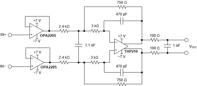
GUID-C6DE7AB1-5276-4FD2-88F0-7BA208B72A64-low.gif Figure 9-1 OPA2205 Configured as a DAQ Input Buffer