SBOSA11E March   2020  – December 2023 OPA206 , OPA2206 , OPA4206

PRODUCTION DATA  

  1.   1
  2. Features
  3. Applications
  4. Description
  5. Pin Configuration and Functions
  6. Specifications
    1. 5.1 Absolute Maximum Ratings
    2. 5.2 ESD Ratings
    3. 5.3 Recommended Operating Conditions
    4. 5.4 Thermal Information: OPA206
    5. 5.5 Thermal Information: OPA2206
    6. 5.6 Thermal Information: OPA4206
    7. 5.7 Electrical Characteristics: VS = ±5 V
    8. 5.8 Electrical Characteristics: VS = ±15 V
    9. 5.9 Typical Characteristics
  7. Parameter Measurement Information
    1. 6.1 Typical Specifications and Distributions
  8. Detailed Description
    1. 7.1 Overview
    2. 7.2 Functional Block Diagram
    3. 7.3 Feature Description
      1. 7.3.1 Input Overvoltage Protection
      2. 7.3.2 Input Offset Trimming
      3. 7.3.3 Lower Input Bias With Super-Beta Inputs
      4. 7.3.4 Overload Power Limiter
      5. 7.3.5 EMI Rejection
    4. 7.4 Device Functional Modes
  9. Application and Implementation
    1. 8.1 Application Information
    2. 8.2 Typical Applications
      1. 8.2.1 Voltage Attenuator
        1. 8.2.1.1 Design Requirements
        2. 8.2.1.2 Detailed Design Procedure
        3. 8.2.1.3 Application Curves
      2. 8.2.2 Discrete, Two-Op-Amp Instrumentation Amplifier
      3. 8.2.3 Input Buffer and Protection for ADC Driver
    3. 8.3 Power Supply Recommendations
    4. 8.4 Layout
      1. 8.4.1 Layout Guidelines
      2. 8.4.2 Layout Example
  10. Device and Documentation Support
    1. 9.1 Device Support
      1. 9.1.1 Development Support
        1. 9.1.1.1 PSpice® for TI
    2. 9.2 Documentation Support
      1. 9.2.1 Related Documentation
    3. 9.3 Receiving Notification of Documentation Updates
    4. 9.4 Support Resources
    5. 9.5 Trademarks
    6. 9.6 Electrostatic Discharge Caution
    7. 9.7 Glossary
  11. 10Revision History
  12. 11Mechanical, Packaging, and Orderable Information

Package Options

Refer to the PDF data sheet for device specific package drawings

Mechanical Data (Package|Pins)
  • D|8
Thermal pad, mechanical data (Package|Pins)
Orderable Information

Input Buffer and Protection for ADC Driver

Section 8.2.1.1 shows the OPA2206 configured as an input buffer for an ADC driver using the THP210. The high dc precision and low noise of the OPA2206 make this device an excellent choice for precision signal chain conditioning. The low input bias of the amplifier minimizes dc errors created for higher output impedance sensors. The integrated input overvoltage protection prevents damage to the signal chain due to an input fault condition where the signal exceeds the supply range of the OPA2206, or if the inputs are shorted to a higher supply rail. For more information on designing a precision ADC driver, see the THP210.
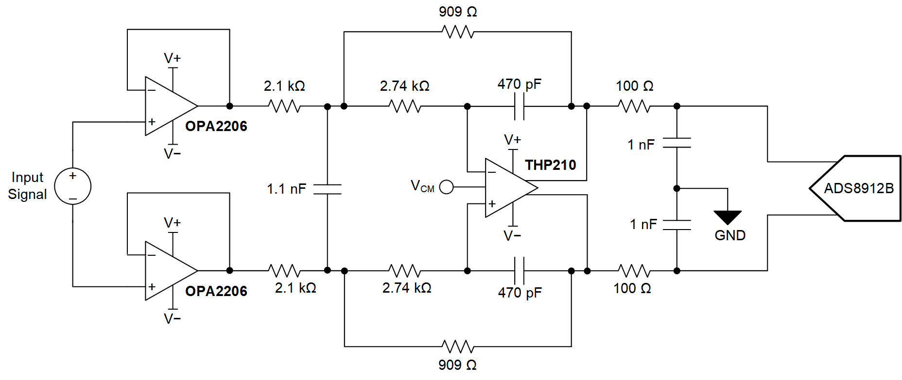
GUID-20210323-CA0I-LP8S-KCVX-R165XH6GTXFB-low.png Figure 8-5 OPA2206 Configured as an Input-Signal-Chain Buffer