SBOS924H September 2018 – August 2021 OPA210 , OPA2210
PRODUCTION DATA
- 1 Features
- 2 Applications
- 3 Description
- 4 Revision History
- 5 Pin Configuration and Functions
- 6 Specifications
- 7 Detailed Description
- 8 Application and Implementation
- 9 Power Supply Recommendations
- 10Layout
- 11Device and Documentation Support
- 12Mechanical, Packaging, and Orderable Information
Package Options
Mechanical Data (Package|Pins)
Thermal pad, mechanical data (Package|Pins)
Orderable Information
8.3.1 Time Gain Control System for Ultrasound Applications
During an ultrasound send-receive cycle, the magnitude of reflected signal depends on the depth of penetration. The ultrasound signal incident on the receiver decreases in amplitude as a function of the time elapsed since transmission. The time gain control (TGC) system helps achieve the best possible signal-to-noise ratio (SNR), even with the decreasing signal amplitude. When the image is displayed, similar materials have similar brightness, regardless of depth. Linear-in-dB gain, which means the decibel gain is a linear function of the control voltage (VCNTL), is used to generate this image.
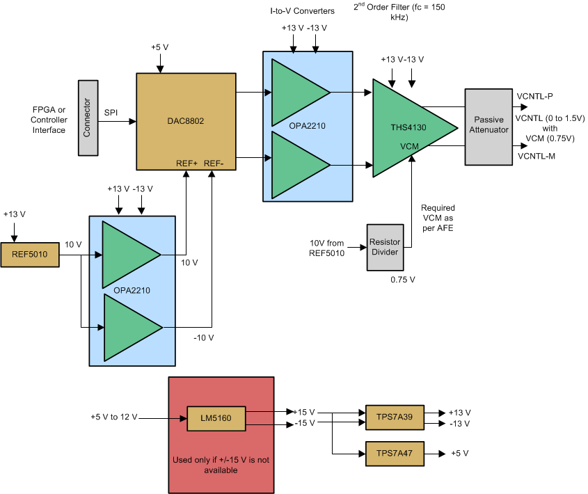
There are multiple approaches for a TGC control circuit that are based on the type of DAC. Figure 8-4 shows a high-level block diagram for the topology using a current-output multiplying DAC (MDAC) to generate the drive for VCNTL. The op amp used for current-to-voltage (I-to-V) conversion must have low-voltage noise, as well as low-current noise density. The current density helps reduce the overall noise performance because of the DAC output configuration. The DAC output can go up to ±10 V; therefore, the op amp must have bipolar operation. The OPAx210 is used here because of the low-voltage noise density of 2.2 nV/√Hz, low-current noise density of 500 fA/√Hz, rail-to-rail output, and the ability to accept a wide supply range of ±2.25 V to ±18 V and provide rail-to-rail output. The low offset voltage and offset drift of the OPAx210 facilitate excellent dc accuracy for the circuit.
The OPAx210 is used to filter and buffer the 10-V reference voltage generated by the REF5010. The REF5010 serves as the reference voltage for the DAC8802, which generates a current output on IOUT corresponding to the digital input code. The IOUT pin of the DAC8802 is connected to the virtual ground (negative terminal) of the OPAx210; the feedback resistor (RFB is internal to the DAC8802) is connected to the output of the OPAx210, and results in a current-to-voltage conversion. The output of the OPAx210 has a range of –10 V to 0 V, which is fed to the THS4130 configured as a Sallen-Key filter. Finally, the 10-V range is attenuated down to a 1.5-V range, with a common-mode voltage of 0.75 V using a resistive attenuator. See the 2.3-nV/√Hz, Differential, Time Gain Control DAC Reference Design for Ultrasound for an in-depth analysis of Figure 8-4.
 Figure 8-4 Block Diagram for Time Gain Control
System for Ultrasound