SBOS809A November 2016 – June 2017 OPA2172-Q1 , OPA4172-Q1
PRODUCTION DATA.
- 1 Features
- 2 Applications
- 3 Description
- 4 Revision History
- 5 Device Comparison Table
- 6 Pin Configuration and Functions
- 7 Specifications
- 8 Detailed Description
- 9 Applications and Implementation
- 10Power Supply Recommendations
- 11Layout
- 12Device and Documentation Support
- 13Mechanical, Packaging, and Orderable Information
Package Options
Mechanical Data (Package|Pins)
- DGK|8
Thermal pad, mechanical data (Package|Pins)
Orderable Information
9 Applications and Implementation
NOTE
Information in the following applications sections is not part of the TI component specification, and TI does not warrant its accuracy or completeness. TI’s customers are responsible for determining suitability of components for their purposes. Customers should validate and test their design implementation to confirm system functionality.
9.1 Application Information
The OPAx172-Q1 family of amplifiers is specified for operation from 4.5 V to 36 V (±2.25 V to ±18 V). Many of the specifications apply from –40°C to +125°C. Parameters that can exhibit significant variance with regard to operating voltage or temperature are presented in the Typical Characteristics section.
9.2 Typical Applications
The following application examples highlight only a few of the circuits where the OPAx172-Q1 can be used.
9.2.1 Capacitive Load Drive Solution Using an Isolation Resistor
The OPA172-Q1 can be used capacitive loads such as cable shields, reference buffers, MOSFET gates, and diodes. The circuit uses an isolation resistor (RISO) to stabilize the output of an op amp. RISO modifies the open-loop gain of the system to ensure the circuit has sufficient phase margin, as shown in Figure 47.
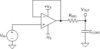 Figure 47. Unity-Gain Buffer with RISO Stability Compensation
9.2.1.1 Design Requirements
The design requirements are:
- Supply voltage: 30 V (±15 V)
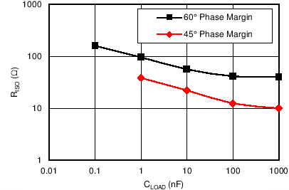
- Capacitive loads: 100 pF, 1000 pF, 0.01 μF, 0.1 μF, and 1 μF
- Phase margin: 45° and 60°
9.2.1.2 Detailed Design Procedure
Figure 47 depicts a unity-gain buffer driving a capacitive load. Equation 1 shows the transfer function for the circuit in Figure 47. Not depicted in Figure 47 is the open-loop output resistance of the op amp, Ro.

The transfer function in Equation 1 has a pole and a zero. The frequency of the pole (fp) is determined by (Ro + RISO) and CLOAD. Components RISO and CLOAD determine the frequency of the zero (fz). A stable system is obtained by selecting RISO such that the rate of closure (ROC) between the open-loop gain (AOL) and 1 / β is 20 dB per decade. Figure 48 shows the concept. Note that the 1 / β curve for a unity-gain buffer is 0 dB.
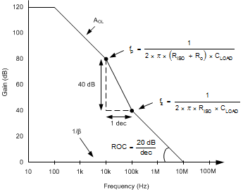 Figure 48. Unity-Gain Amplifier with RISO Compensation
ROC stability analysis is typically simulated. The validity of the analysis depends on multiple factors, especially the accurate modeling of Ro. In addition to simulating the ROC, a robust stability analysis includes a measurement of overshoot percentage and ac gain peaking of the circuit using a function generator, oscilloscope, and gain and phase analyzer. Phase margin is then calculated from these measurements. Table 5 shows the overshoot percentage and ac gain peaking that correspond to phase margins of 45° and 60°. For more details on this design and other alternative devices that can be used in place of the OPA172-Q1, see the Capacitive Load Drive Solution using an Isolation Resistorprecision design (TIPD128).
Table 5. Phase Margin versus Overshoot and AC Gain Peaking
| PHASE MARGIN | OVERSHOOT | AC GAIN PEAKING |
|---|---|---|
| 45° | 23.3% | 2.35 dB |
| 60° | 8.8% | 0.28 dB |
9.2.2 Bidirectional Current Source
The improved Howland current-pump topology shown in Figure 50 provides excellent performance because of the extremely tight tolerances of the on-chip resistors of the INA132. By buffering the output using an OPA172-Q1, the output current the circuit is able to deliver is greatly extended.
The circuit dc transfer function is shown in Equation 2.
The OPA172-Q1 can also be used as the feedback amplifier because the low bias current minimizes error voltages produced across R1. However, for improved performance, select a FET-input device with extremely low offset, such as the OPA192, OPA140, or OPA188 as the feedback amplifier.
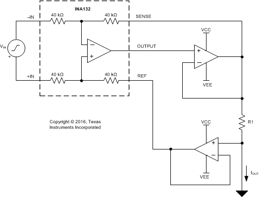 Figure 50. Bidirectional Current Source
9.2.3 JFET-Input Low-Noise Amplifier
Figure 51 shows a low-noise composite amplifier built by adding a low noise JFET pair (Q1 and Q2) as an input preamplifier for the OPA172-Q1. Transistors Q3 and Q4 form a 2-mA current sink that biases each JFET with 1 mA of drain current. Using 3.9-kΩ drain resistors produces a gain of approximately 10 in the input amplifier, making the extremely-low, broadband-noise spectral density of the JFET pair, Q1 and Q2, the dominant noise source of the amplifier. The output impedance of the input differential amplifier is large enough that a FET-input amplifier such as the OPA172-Q1 provides superior noise performance over bipolar-input amplifiers.
The gain of the composite amplifier is given by Equation 3.
The resistances shown are standard 1% resistor values that produce a gain of approximately 100 (99.26) with 68° of phase margin. Gains less than 10 may require additional compensation methods to provide stability. Select low resistor values to minimize the resistor thermal noise contribution to the total output noise.
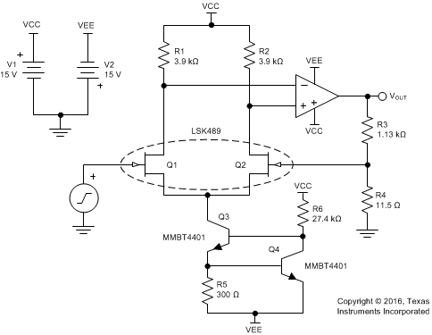 Figure 51. JFET-Input Low-Noise Amplifier
