SBOS962F April 2020 – March 2023 OPA205 , OPA2205 , OPA4205
PRODMIX
- 1 Features
- 2 Applications
- 3 Description
- 4 Revision History
- 5 Pin Configuration and Functions
- 6 Specifications
- 7 Parameter Measurement Information
- 8 Detailed Description
- 9 Application and Implementation
- 10Device and Documentation Support
- 11Mechanical, Packaging, and Orderable Information
Package Options
Mechanical Data (Package|Pins)
Thermal pad, mechanical data (Package|Pins)
Orderable Information
8.3.1 Input Offset Trimming
The OPAx205 are the industry's first e-trim operational amplifiers built on a bipolar process. The input offset voltage of an amplifier is determined by the inherent mismatch between the input transistors. The offset can be minimized using laser-trimming performed during the manufacturing process while the devices are still in the bare silicon form. However, when the silicon is packaged, the packaging process introduces additional offset due to mechanic stresses. TI's new trimming processes are used to trim the offset after the packaging process is complete to minimize both inherent and package-induced offsets. After trimming, communication is disabled to make sure the amplifiers operate properly in the final system.
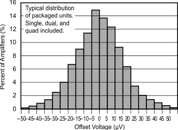
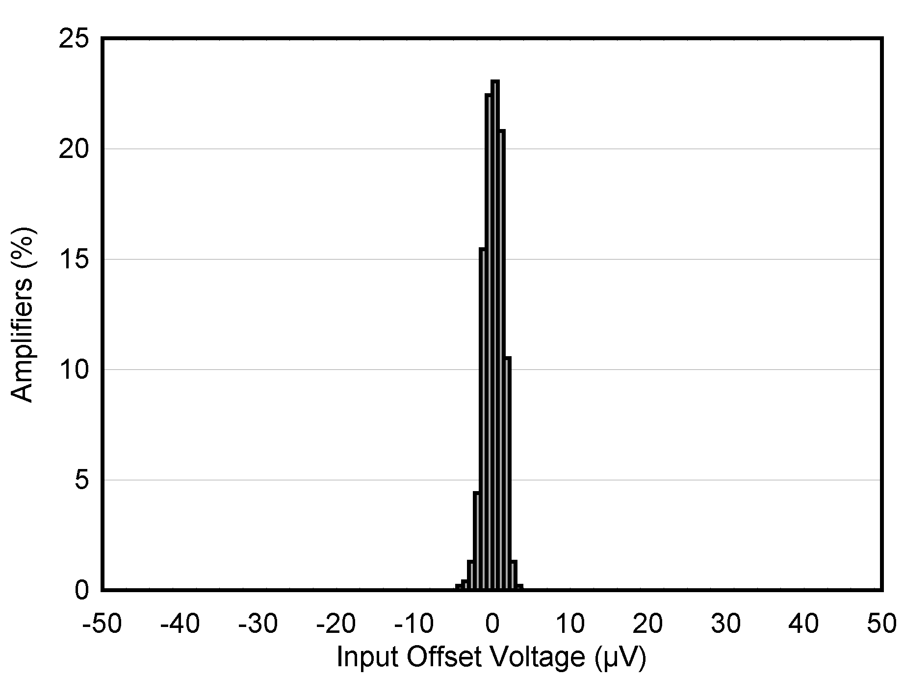
A comparison between production offset values for the industry-popular, laser-trimmed OPA2277 and the OPAx205 proprietary trim can be seen in Figure 8-1 and Figure 8-2.
 Figure 8-1 OPA2277 Laser-Trimmed Operational Amplifier Offset
 Figure 8-2 OPAx205 e-trim™
Operational Amplifier Offset
Figure 8-2 OPAx205 e-trim™
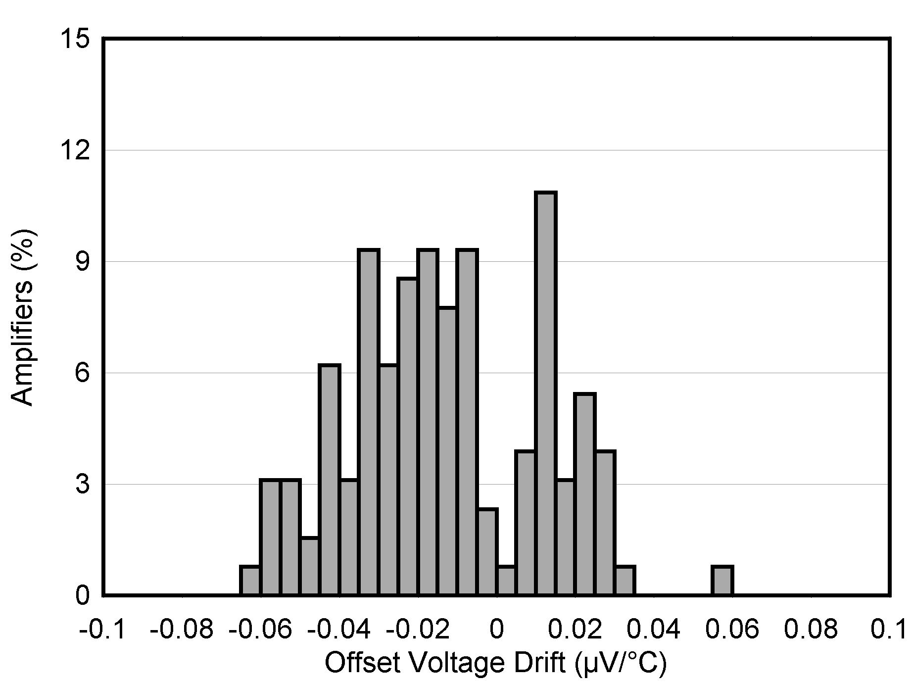
Operational Amplifier OffsetThe OPAx205 are also trimmed at two temperatures to minimize the input offset voltage drift over temperature. The final performance of the offset drift can be seen in Figure 8-3.
 Figure 8-3 OPAx205 e-trim™
Operational Amplifier Drift