SLOS884B September 2014 – December 2018 OPA2320-Q1 , OPA320-Q1
PRODUCTION DATA.
- 1 Features
- 2 Applications
- 3 Description
- 4 Revision History
- 5 Pin Configuration and Functions
- 6 Specifications
- 7 Detailed Description
- 8 Application and Implementation
- 9 Power Supply Recommendations
- 10Layout
- 11Device and Documentation Support
- 12Mechanical, Packaging, and Orderable Information
Package Options
Mechanical Data (Package|Pins)
- DGK|8
Thermal pad, mechanical data (Package|Pins)
Orderable Information
8.2.4 Active Filter
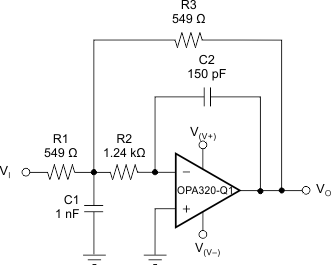
The OPAx320-Q1 is an excellent choice for active filter applications that require a wide bandwidth, fast slew rate, low-noise, single-supply operational amplifier. Figure 43 shows a 500 kHz, second-order, low-pass filter using the multiple-feedback (MFB) topology. The components have been selected to provide a maximally-flat Butterworth response. Beyond the cutoff frequency, roll-off is –40 dB/dec. The Butterworth response is excellent for applications requiring predictable gain characteristics, such as the antialiasing filter used in front of an ADC.
One point to observe when considering the MFB filter is that the output is inverted, relative to the input. If this inversion is not required, or not desired, a noninverting output can be achieved through one of the following options:
- adding an inverting amplifier
- adding an additional second-order MFB stage
- using a noninverting filter topology, such as the Sallen-Key
 Figure 43. Second-Order Butterworth 500-kHz Low-Pass Filter
  Figure 44. OPAx320-Q1 Configured as a Three-Pole, 20-kHz, Sallen-Key Filter