SBOS513F August 2010 – December 2016 OPA2320 , OPA320
PRODUCTION DATA.
- 1 Features
- 2 Applications
- 3 Description
- 4 Revision History
- 5 Pin Configuration and Functions
- 6 Specifications
-
7 Detailed Description
- 7.1 Overview
- 7.2 Functional Block Diagram
- 7.3
Feature Description
- 7.3.1 Operating Voltage
- 7.3.2 Input and ESD Protection
- 7.3.3 Rail-to-Rail Input
- 7.3.4 Phase Reversal
- 7.3.5 Feedback Capacitor Improves Response
- 7.3.6 EMI Susceptibility and Input Filtering
- 7.3.7 Output Impedance
- 7.3.8 Capacitive Load and Stability
- 7.3.9 Overload Recovery Time
- 7.3.10 Shutdown Function
- 7.3.11 Leadless SON Package
- 7.4 Device Functional Modes
- 8 Application and Implementation
- 9 Power Supply Recommendations
- 10Layout
- 11Device and Documentation Support
- 12Mechanical, Packaging, and Orderable Information
Package Options
Mechanical Data (Package|Pins)
Thermal pad, mechanical data (Package|Pins)
- DRG|8
Orderable Information
1 Features
- Precision with Zero-Crossover Distortion:
- Low Offset Voltage: 150 µV (Maximum)
- High CMRR: 114 dB
- Rail-to-Rail I/O
- Low Input Bias Current: 0.9 pA (Maximum)
- Low Noise: 7 nV/√Hz at 10 kHz
- Wide Bandwidth: 20 MHz
- Slew Rate: 10 V/µs
- Quiescent Current: 1.45 mA/Ch
- Single-Supply Voltage Range: 1.8 V to 5.5 V
- OPA320S and OPA2320S:
- IQ in Shutdown Mode: 0.1 µA
- Unity-Gain Stable
- Small Packages:
- SOT-23, VSSOP, SON, and SOIC
2 Applications
- High-Z Sensor Signal Conditioning
- Transimpedance Amplifiers
- Test and Measurement Equipment
- Programmable Logic Controllers (PLCs)
- Motor Control Loops
- Communications
- Input/Output ADC/DAC Buffers
- Active Filters
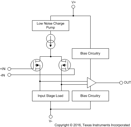
Block Diagram

3 Description
The OPA320 (single) and OPA2320 (dual) are a new generation of precision, low-voltage CMOS operational amplifiers optimized for very low noise and wide bandwidth while operating on a low quiescent current of only 1.45 mA.
The OPA320 series is ideal for low-power, single-supply applications. Low-noise (7 nV/√Hz) and high-speed operation also make them well-suited for driving sampling analog-to-digital converters (ADCs). Other applications include signal conditioning and sensor amplification.
The OPA320 features a linear input stage with zero-crossover distortion that delivers excellent common-mode rejection ratio (CMRR) of typically 114 dB over the full input range. The input common mode range extends 100 mV beyond the negative and positive supply rails. The output voltage typically swings within 10 mV of the rails.
In addition, the OPAx320 has a wide supply voltage range from 1.8 V to 5.5 V with excellent PSRR
(106 dB) over the entire supply range, making them suitable for precision, low-power applications that run directly from batteries without regulation.
The OPA320 (single version) is available in a 5-pin SOT23 package; the OPA320S shutdown single version is available in an 6-pin SOT23 package. The dual OPA2320 is offered in 8-pin SOIC, VSSOP, and SON packages, and the OPA2320S (dual with shutdown) in a 10-pin VSSOP package.
Device Information(1)
| PART NUMBER | PACKAGE | BODY SIZE (NOM) |
|---|---|---|
| OPA320 | SOT-23 (5) | 2.90 mm × 1.60 mm |
| OPA320S | SOT-23 (6) | 2.90 mm × 1.60 mm |
| OPA2320 | VSSOP (8) | 3.00 mm × 3.00 mm |
| SOIC (8) | 4.90 mm × 3.91 mm | |
| SON (10) | 3.00 mm × 3.00 mm | |
| OPA2320S | VSSOP (10) | 3.00 mm × 3.00 mm |
- For all available packages, see the orderable addendum at the end of the data sheet.
4 Revision History
Changes from E Revision (June 2013) to F Revision
- Added ESD Ratings table, Feature Description section, Device Functional Modes, Application and Implementation section, Power Supply Recommendations section, Layout section, Device and Documentation Support section, and Mechanical, Packaging, and Orderable Information section Go
- Changed package families throughout data sheet: DFN to SON, MSOP to VSSOP, and SO to SOICGo
Changes from D Revision (November 2011) to E Revision
- Deleted Ordering Information tableGo
- Changed Shutdown, VIH and VIL parameters in Electrical Characteristics tableGo
- Added Figure 29 and Figure 30Go
- Added Figure 31 and Figure 32Go
Changes from C Revision (August 2011) to D Revision
- Changed status of OPA2320 SO-8 (D) to production data from product preview.Go
Changes from B Revision (March 2010) to C Revision
- Deleted D (SO-8) package pinout drawing from Pin Configurations and FunctionsGo
- Changed names of pins 2 and 6 for DGS (MSOP-10) package Go
- Added values to Thermal Information tables, moved to new page, and updated formatGo
- Added SHDN value to Electrical Characteristics condition lineGo
- Added new test condition row for Input Bias Current Over Temperature parameterGo
- Changed test condition for Phase Margin parameter in Electrical CharacteristicsGo
- Added test condition to Short-Circuit Current parameter in Electrical CharacteristicsGo
- Changed Shutdown subsection of Electrical Characteristics along with associated notesGo
- Changed Power Supply subsection of Electrical CharacteristicsGo
- Changed Figure 4Go
- Changed Figure 18Go
- Changed 100 µs to 100 ns in first paragraph of Overload Recovery Time sectionGo
- Changed Figure 38Go
- Changed Figure 39Go
- Changed R2 value in Figure 44 from 500Ω to 50kΩGo