SLOS856B June   2013  – May 2017 OPA2322-Q1 , OPA322-Q1 , OPA4322-Q1

PRODUCTION DATA.  

  1. Features
  2. Applications
  3. Description
  4. Revision History
  5. Pin Configuration and Functions
  6. Specifications
    1. 6.1 Absolute Maximum Ratings
    2. 6.2 ESD Ratings
    3. 6.3 Recommended Operating Conditions
    4. 6.4 Thermal Information: OPA322-Q1
    5. 6.5 Thermal Information: OPA2322-Q1
    6. 6.6 Thermal Information: OPA4322-Q1
    7. 6.7 Electrical Characteristics
  7. Typical Characteristics
  8. Detailed Description
    1. 8.1 Overview
    2. 8.2 Functional Block Diagram
    3. 8.3 Feature Description
      1. 8.3.1 Operating Voltage
      2. 8.3.2 Input and ESD Protection
      3. 8.3.3 Phase Reversal
      4. 8.3.4 Feedback Capacitor Improves Response
      5. 8.3.5 EMI Susceptibility and Input Filtering
      6. 8.3.6 Output Impedance
      7. 8.3.7 Capacitive Load and Stability
      8. 8.3.8 Overload Recovery Time
    4. 8.4 Device Functional Modes
  9. Application and Implementation
    1. 9.1 Application Information
      1. 9.1.1 Active Filter
    2. 9.2 Typical Application
      1. 9.2.1 Design Requirements
      2. 9.2.2 Detailed Design Procedure
      3. 9.2.3 Application Curve
  10. 10Power Supply Recommendations
  11. 11Layout
    1. 11.1 Layout Guidelines
    2. 11.2 Layout Example
  12. 12Device and Documentation Support
    1. 12.1 Device Support
      1. 12.1.1 Third-Party Products Disclaimer
      2. 12.1.2 Development Support
        1. 12.1.2.1 TINA-TI™ (Free Software Download)
        2. 12.1.2.2 DIP Adapter EVM
        3. 12.1.2.3 Universal Operational Amplifier EVM
        4. 12.1.2.4 TI Precision Designs
        5. 12.1.2.5 WEBENCH Filter Designer
    2. 12.2 Documentation Support
      1. 12.2.1 Related Documentation
    3. 12.3 Related Links
    4. 12.4 Receiving Notification of Documentation Updates
    5. 12.5 Community Resources
    6. 12.6 Trademarks
    7. 12.7 Electrostatic Discharge Caution
    8. 12.8 Glossary
  13. 13Mechanical, Packaging, and Orderable Information

Package Options

Mechanical Data (Package|Pins)
Thermal pad, mechanical data (Package|Pins)
Orderable Information

Typical Characteristics

at TA = 25°C, VCM = VOUT = midsupply, and RL = 10 kΩ (unless otherwise noted)
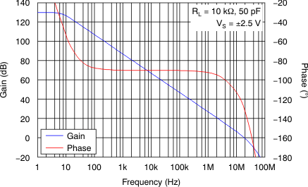
OPA322-Q1 OPA2322-Q1 OPA4322-Q1 tc_oloop_g_ph-frq_bos538.gif
Figure 1. Open-Loop Gain and Phase vs Frequency
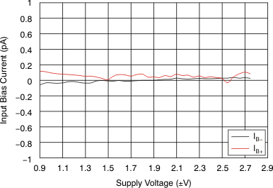
OPA322-Q1 OPA2322-Q1 OPA4322-Q1 tc_ibc-vs_bos513.gif Figure 3. Input Bias Current vs Supply Voltage
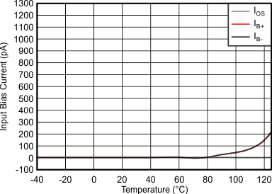
OPA322-Q1 OPA2322-Q1 OPA4322-Q1 tc_ibc-tmp_bos538.gif
Figure 5. Input Bias Current vs Temperature
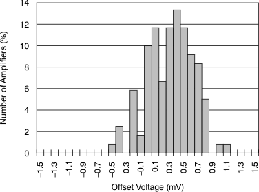
OPA322-Q1 OPA2322-Q1 OPA4322-Q1 tc_histo_voff_bos538.gif
Figure 7. Offset Voltage Production Histogram
OPA322-Q1 OPA2322-Q1 OPA4322-Q1 tc_noise_density_bos538.gif
Figure 9. Input Voltage Noise Spectral Density
vs Frequency
OPA322-Q1 OPA2322-Q1 OPA4322-Q1 tc_cloop-frq_18v_bos538.gif Figure 11. Closed-Loop Gain vs Frequency
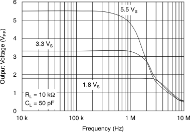
OPA322-Q1 OPA2322-Q1 OPA4322-Q1 tc_max_vo-frq_bos538.gif Figure 13. Maximum Output Voltage vs Frequency
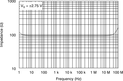
OPA322-Q1 OPA2322-Q1 OPA4322-Q1 tc_oloop_imp-frq_bos538.gif Figure 15. Open-Loop Output Impedance
vs Frequency
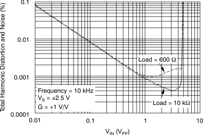
OPA322-Q1 OPA2322-Q1 OPA4322-Q1 tc_thdn-amp_bos538.gif Figure 17. THD+N vs Amplitude
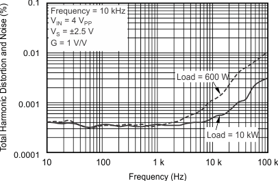
OPA322-Q1 OPA2322-Q1 OPA4322-Q1 tc_thdn-frq_4vin_bos538.gif Figure 19. THD+N vs Frequency
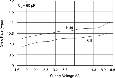
OPA322-Q1 OPA2322-Q1 OPA4322-Q1 tc_sr-vs_bos538.gif Figure 21. Slew Rate vs Supply Voltage
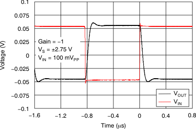
OPA322-Q1 OPA2322-Q1 OPA4322-Q1 tc_sm_step_neg_bos538.gif Figure 23. Small-Signal Step Response
OPA322-Q1 OPA2322-Q1 OPA4322-Q1 tc_cmrr_psrr-frq_bos538.gif Figure 25. CMRR and PSRR vs Frequency
OPA322-Q1 OPA2322-Q1 OPA4322-Q1 tc_oloop_g-tmp_bos538.gif
Figure 2. Open-Loop Gain vs Temperature
OPA322-Q1 OPA2322-Q1 OPA4322-Q1 tc_ibc-vcm_bos513.gif Figure 4. Input Bias Current
vs Common-Mode Voltage
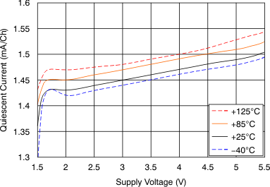
OPA322-Q1 OPA2322-Q1 OPA4322-Q1 tc_iq-vs_bos538.gif
Figure 6. Quiescent Current vs Supply Voltage Per Amplifier
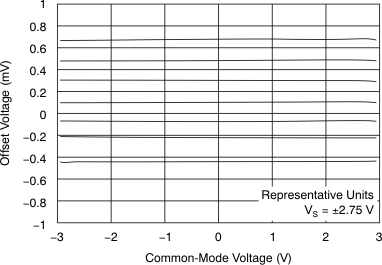
OPA322-Q1 OPA2322-Q1 OPA4322-Q1 tc_voff-vcm_bos538.gif
Figure 8. Offset Voltage vs Common-Mode Voltage
OPA322-Q1 OPA2322-Q1 OPA4322-Q1 tc_vin_noise_bos538.gif
Figure 10. 0.1-Hz to 10-Hz Input Voltage Noise
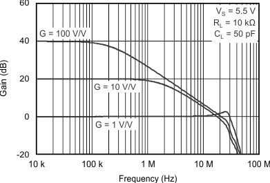
OPA322-Q1 OPA2322-Q1 OPA4322-Q1 tc_cloop-frq_55v_bos538.gif Figure 12. Closed-Loop Gain vs Frequency
OPA322-Q1 OPA2322-Q1 OPA4322-Q1 tc_vo-io_bos538.gif Figure 14. Output Voltage Swing vs Output Current
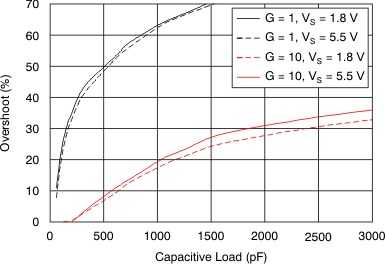
OPA322-Q1 OPA2322-Q1 OPA4322-Q1 tc_oshoot-cl_bos538.gif Figure 16. Small-Signal Overshoot
vs Load Capacitance
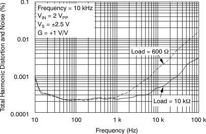
OPA322-Q1 OPA2322-Q1 OPA4322-Q1 tc_thdn-frq_2vin_bos538.gif Figure 18. THD+N vs Frequency
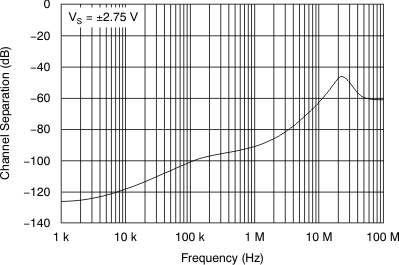
OPA322-Q1 OPA2322-Q1 OPA4322-Q1 tc_ch_sep-frq_bos538.gif Figure 20. Channel Separation
vs Frequency (Dual-Channel)
OPA322-Q1 OPA2322-Q1 OPA4322-Q1 tc_sm_step_pos_bos538.gif Figure 22. Small-Signal Step Response
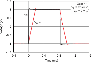
OPA322-Q1 OPA2322-Q1 OPA4322-Q1 tc_lg_step_resp_bos538.gif Figure 24. Large-Signal Step Response vs Time