SBOS465C January 2009 – January 2016 OPA2348-Q1 , OPA348-Q1 , OPA4348-Q1
PRODUCTION DATA.
- 1 Features
- 2 Applications
- 3 Description
- 4 Revision History
- 5 Pin Configuration and Functions
- 6 Specifications
- 7 Detailed Description
- 8 Application and Implementation
- 9 Power Supply Recommendations
- 10Layout
- 11Device and Documentation Support
- 12Mechanical, Packaging, and Orderable Information
Package Options
Mechanical Data (Package|Pins)
- D|8
Thermal pad, mechanical data (Package|Pins)
Orderable Information
7 Detailed Description
7.1 Overview
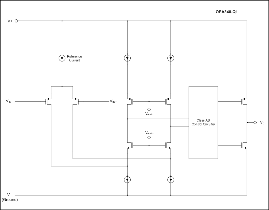
The OPAx348-Q1 family of devices is a low-power, rail-to-rail input and output operational amplifier. These devices operate from 1.8 V to 5.5 V, are unity-gain stable, and are suitable for a wide range of general-purpose applications. The class AB output stage is capable of driving ≤ 10-kΩ loads connected to any point between V+ and ground. The input common-mode voltage range includes both rails and allows the OPAx348-Q1 family of devices to be used in virtually any single-supply application. Rail-to-rail input and output swing significantly increases dynamic range, especially in low-supply applications, and makes them ideal for driving sampling analog-to-digital converters (ADCs).
7.2 Functional Block Diagram
7.3 Feature Description
7.3.1 Operating Voltage
The OPAx348-Q1 op amp is fully specified and ensured for operation from 1.8 V to 5.5 V. In addition, many specifications apply from –40°C to +125°C. Parameters that vary significantly with operating voltages or temperature are shown in the Typical Characteristics graphs. Power-supply pins should be bypassed with
0.01-μF ceramic capacitors.
7.3.2 Rail-to-Rail Input
The input common-mode voltage range of the OPAx348-Q1 family of devices extends 200 mV beyond the supply rails. This performance is achieved with a complementary input stage: an N-channel input differential pair in parallel with a P-channel differential pair. The N-channel pair is active for input voltages close to the positive rail, typically (V+) – 1.3 V to 200 mV above the positive supply. The P-channel pair is on for inputs from 200 mV below the negative supply to approximately (V+) – 1.3 V. A small transition region exists, typically (V+) – 1.4 V to (V+) – 1.2 V, in which both pairs are on. This 200-mV transition region can vary up to 300 mV with process variation. Thus, the transition region (both stages on) can range from (V+) – 1.7 V to (V+) – 1.5 V on the low end, up to (V+) – 1.1 V to (V+) – 0.9 V on the high end. Within this transition region, PSRR, CMRR, offset voltage, offset drift, and THD may be degraded compared to device operation outside this region.
7.3.3 Rail-to-Rail Input
The input common-mode range extends from (V–) – 0.2 V to (V+) + 0.2 V. For normal operation, the inputs should be limited to this range. The absolute maximum input voltage is 500 mV beyond the supplies. Inputs greater than the input common-mode range but less than the maximum input voltage, while not valid, do not cause any damage to the op amp. Unlike some other op amps, if the input current is limited, the inputs may go beyond the power supplies without phase inversion, as shown in Figure 19.
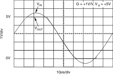 Figure 19. No Phase Inversion with Inputs Greater Than Power-Supply Voltage
Normally, input currents are 0.5 pA. However, large inputs (greater than 500 mV beyond the supply rails) can cause excessive current to flow in or out of the input pins. Therefore, limiting the input current to less than 10 mA is important as well as keeping the input voltage below the maximum rating. This limiting is easily accomplished with an input voltage resistor, as shown in Figure 20.
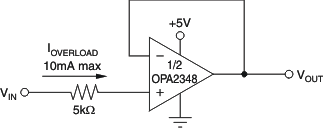 Figure 20. Input Current Protection for Voltages Exceeding the Supply Voltage
7.3.4 Input and ESD Protection
The OPAx348-Q1 family of devices incorporates internal electrostatic discharge (ESD) protection circuits on all pins. In the case of input and output pins, this protection primarily consists of current-steering diodes connected between the input and power-supply pins. These ESD protection diodes also provide in-circuit, input overdrive protection, as long as the current is limited to 10 mA as stated in the Absolute Maximum Ratings table. Figure 21 shows how a series input resistor can be added to the driven input to limit the input current. The added resistor contributes thermal noise at the amplifier input and the value should be kept to a minimum in noise-sensitive applications.
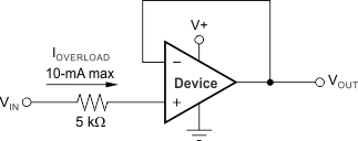 Figure 21. Input Current Protection
7.3.5 Common-Mode Rejection Ratio (CMRR)
CMRR for the OPAx348-Q1 family of devices is specified in several ways so the best match for a given application may be used; see the Electrical Characteristics table. First, the CMRR of the device in the common-mode range below the transition region [VCM < (V+) – 1.3 V] is given. This specification is the best indicator of the capability of the device when the application requires use of one of the differential input pairs. Second, the CMRR over the entire common-mode range is specified at (VCM = –0.2 V to 5.7 V). This last value includes the variations seen through the transition region (see Figure 22).
7.3.6 Common-Mode Voltage Range
The input common-mode voltage range of the OPAx348-Q1 device extends 200 mV beyond the supply rails. This extended range is achieved with a complementary input stage—an N-channel input differential pair in parallel with a P-channel differential pair. The N-channel pair is active for input voltages close to the positive rail, typically (V+) – 1.2 V to 300 mV above the positive supply, while the P-channel pair is on for inputs from 300 mV below the negative supply to approximately (V+) – 1.4 V. A small transition region exists, typically (V+) – 1.4 V to (V+) – 1.2 V, in which both pairs are on. This 200-mV transition region, shown in Figure 22, can vary ±300 mV with process variation. Thus, the transition region (both stages on) can range from (V+) – 1.7 V to (V+) – 1.5 V on the low end, up to (V+) – 1.1 V to (V+) – 0.9 V on the high end. Within the 200-mV transition region, PSRR, CMRR, offset voltage, offset drift, and THD may be degraded compared to operation outside this region.
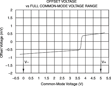 Figure 22. Behavior of Typical Transition Region at Room Temperature
7.3.7 EMI Susceptibility and Input Filtering
Op amps vary with regard to the susceptibility of the device to electromagnetic interference (EMI). If conducted EMI enters the op amp, the dc offset observed at the amplifier output may shift from the nominal value while EMI is present. This shift is a result of signal rectification associated with the internal semiconductor junctions. While all op amp pin functions can be affected by EMI, the signal input pins are likely to be the most susceptible. The OPAx348-Q1 family of devices incorporates an internal input, low-pass filter that reduces the amplifier response to EMI. Both common-mode and differential mode filtering are provided by this filter. The filter is designed for a cutoff frequency of approximately 80 MHz (–3 dB), with a roll-off of 20 dB per decade.
Texas Instruments has developed the ability to accurately measure and quantify the immunity of an operational amplifier over a broad frequency spectrum extending from 10 MHz to 6 GHz. The EMI rejection ratio (EMIRR) metric allows op amps to be directly compared by the EMI immunity. Detailed information can also be found in the application report, EMI Rejection Ratio of Operational Amplifiers (SBOA128), available for download from www.ti.com.
7.3.8 Rail-to-Rail Output
Designed as a micro-power, low-noise operational amplifier, the OPAx348-Q1 family of devices delivers a robust output drive capability. A class AB output stage with common-source transistors is used to achieve full rail-to-rail output swing capability. For resistive loads up to 10 kΩ, the output swings typically to within 5 mV of either supply rail regardless of the power-supply voltage applied. Different load conditions change the ability of the amplifier to swing close to the rails; refer to the graph, Output Voltage Swing vs Output Current.
A class AB output stage with common-source transistors is used to achieve rail-to-rail output. This output stage is capable of driving 5-kΩ loads connected to any potential between V+ and ground. For light resistive loads (>100 kΩ), the output voltage can typically swing to within 18 mV from supply rail. With moderate resistive loads (10 kΩ to 50 kΩ), the output voltage can typically swing to within 100 mV of the supply rails while maintaining high open-loop gain (see Figure 6 in the Typical Characteristics section).
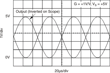 Figure 23. Rail-to-Rail I/O
7.3.9 Capacitive Load and Stability
The OPAx348-Q1 family of devices in a unity-gain configuration can directly drive up to 250-pF pure capacitive load. Increasing the gain enhances the ability of the amplifier to drive greater capacitive loads (see Figure 13 in the Typical Characteristics section). In unity-gain configurations, capacitive load drive can be improved by inserting a small (10-Ω to 20-Ω) resistor, RS, in series with the output, as shown in Figure 24. This resistor significantly reduces ringing while maintaining dc performance for purely capacitive loads. However, if a resistive load exists in parallel with the capacitive load, a voltage divider is created, introducing a direct current (dc) error at the output and slightly reducing the output swing. The error introduced is proportional to the ratio RS/RL and is generally negligible.
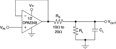 Figure 24. Series Resistor in Unity-Gain Buffer Configuration Improves Capacitive Load Drive
In unity-gain inverter configuration, the phase margin can be reduced by the reaction between the capacitance at the op amp input and the gain setting resistors, thus degrading capacitive load drive. The best performance is achieved by using small-valued resistors. For example, when driving a 500-pF load, reducing the resistor values from 100 kΩ to 5 kΩ decreases overshoot from 55% to 13% (see Figure 13 in the Typical Characteristics section). However, when large-valued resistors cannot be avoided, a small (4-pF to 6-pF) capacitor, CFB, can be inserted in the feedback loop, as shown in Figure 25. This small capacitor significantly reduces overshoot by compensating the effect of capacitance, CIN, which includes the input capacitance of the amplifier and printed circuit board (PCB) parasitic capacitance.
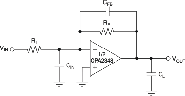 Figure 25. Improving Capacitive Load Drive
7.4 Device Functional Modes
The OPAx348-Q1 family of devices is powered on when the supply is connected. The device can be operated as a single-supply operational amplifier or a dual-supply amplifier, depending on the application.