SBOS235F March 2002 – April 2018 OPA2357 , OPA357
PRODUCTION DATA.
- 1 Features
- 2 Applications
- 3 Description
- 4 Revision History
- 5 Pin Configuration and Functions
- 6 Specifications
-
7 Detailed Description
- 7.1 Overview
- 7.2 Functional Block Diagram
- 7.3
Feature Description
- 7.3.1 OPAx357 Comparison
- 7.3.2 Operating Voltage
- 7.3.3 Enable Function
- 7.3.4 Rail-to-Rail Input
- 7.3.5 Rail-to-Rail Output
- 7.3.6 Output Drive
- 7.3.7 Video
- 7.3.8 Wideband Video Multiplexing
- 7.3.9 Driving Analog-to-Digital Converters
- 7.3.10 Capacitive Load and Stability
- 7.3.11 Wideband Transimpedance Amplifier
- 7.4 Device Functional Modes
- 8 Application and Implementation
- 9 Power Supply Recommendations
- 10Layout
- 11Device and Documentation Support
- 12Mechanical, Packaging, and Orderable Information
Package Options
Mechanical Data (Package|Pins)
- DGS|10
Thermal pad, mechanical data (Package|Pins)
Orderable Information
7.3.7 Video
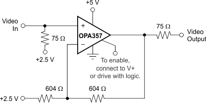
The OPA357 output stage is capable of driving standard back-terminated 75-Ω video cables, as shown in Figure 35. By back-terminating a transmission line, the cable does not exhibit a capacitive load to its driver. A properly back-terminated 75-Ω cable does not appear as capacitance; this cable presents only a 150-Ω resistive load to the OPA357 output.
 Figure 35. Single-Supply Video Line Driver
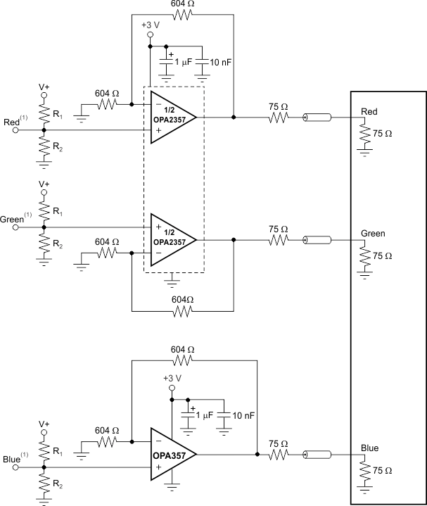
The OPA357 can be used as an amplifier for RGB graphic signals, which have a voltage of zero at the video black level, by offsetting and AC-coupling the signal, as shown in Figure 36.

1. The source video signal offset is 300 mV above ground to accommodate the op amp swing-to-ground capability.
Figure 36. RGB Cable Driver