SBOS673D September 2017 – December 2018 OPA2837 , OPA837
PRODUCTION DATA.
- 1 Features
- 2 Applications
- 3 Description
- 4 Revision History
- 5 Pin Configuration and Functions
-
6 Specifications
- 6.1 Absolute Maximum Ratings
- 6.2 ESD Ratings
- 6.3 Recommended Operating Conditions
- 6.4 Thermal Information: OPA837
- 6.5 Thermal Information: OPA2837
- 6.6 Electrical Characteristics: VS = 5 V
- 6.7 Electrical Characteristics: VS = 3 V
- 6.8 Typical Characteristics: VS = 5.0 V
- 6.9 Typical Characteristics: VS = 3.0 V
- 6.10 Typical Characteristics: ±2.5-V to ±1.5-V Split Supply
- 7 Detailed Description
-
8 Application and Implementation
- 8.1
Application Information
- 8.1.1 Noninverting Amplifier
- 8.1.2 Inverting Amplifier
- 8.1.3 Output DC Error Calculations
- 8.1.4 Output Noise Calculations
- 8.1.5 Instrumentation Amplifier
- 8.1.6 Attenuators
- 8.1.7 Differential to Single-Ended Amplifier
- 8.1.8 Differential-to-Differential Amplifier
- 8.1.9 Pulse Application With Single-Supply Circuit
- 8.1.10 ADC Driver Performance
- 8.2 Typical Applications
- 8.1
Application Information
- 9 Power Supply Recommendations
- 10Layout
- 11Device and Documentation Support
- 12Mechanical, Packaging, and Orderable Information
Package Options
Mechanical Data (Package|Pins)
Thermal pad, mechanical data (Package|Pins)
- RUN|10
Orderable Information
8.1.5 Instrumentation Amplifier
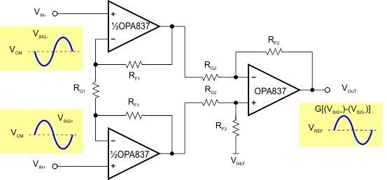
Figure 77 is an instrumentation amplifier that combines the high input impedance of the differential-to-differential amplifier circuit and the common-mode rejection of the differential-to-single-ended amplifier circuit. This circuit is often used in applications where high input impedance is required (such as taps from a differential line) or in cases where the signal source is a high impedance.
 Figure 77. Instrumentation Amplifier (INA)
 The output of the amplifier can be calculated according to Equation 7 if VIN+ = VCM + VSIG+ and VIN– = VCM + VSIG–.

Equation 8 shows the signal gain of the circuit. The input VCM is rejected, and VREF provides a reference voltage or level shift around which the output signal swings. The single-ended output signal is in-phase to the lower input signal polarity.

Integrated INA solutions are available, but the OPAx837 device provides a high-frequency solution at relatively low power (< 1.8 mA for the three op-amp solution). For best CMRR performance, resistors must be matched. A good rule of thumb is CMRR ≈ the resistor tolerance; so a 0.1% tolerance provides approximately 60-dB CMRR. For higher gain INA implementations with higher bandwidths, apply the OPA838 to the circuit of Figure 77.