SBOS513F August   2010  – December 2016 OPA2320 , OPA320

PRODUCTION DATA.  

  1. Features
  2. Applications
  3. Description
  4. Revision History
  5. Pin Configuration and Functions
  6. Specifications
    1. 6.1 Absolute Maximum Ratings
    2. 6.2 ESD Ratings
    3. 6.3 Recommended Operating Conditions
    4. 6.4 Thermal Information: OPA320 and OPA320S
    5. 6.5 Thermal Information: OPA2320
    6. 6.6 Thermal Information: OPA2320S
    7. 6.7 Electrical Characteristics
    8. 6.8 Typical Characteristics
  7. Detailed Description
    1. 7.1 Overview
    2. 7.2 Functional Block Diagram
    3. 7.3 Feature Description
      1. 7.3.1  Operating Voltage
      2. 7.3.2  Input and ESD Protection
      3. 7.3.3  Rail-to-Rail Input
      4. 7.3.4  Phase Reversal
      5. 7.3.5  Feedback Capacitor Improves Response
      6. 7.3.6  EMI Susceptibility and Input Filtering
      7. 7.3.7  Output Impedance
      8. 7.3.8  Capacitive Load and Stability
      9. 7.3.9  Overload Recovery Time
      10. 7.3.10 Shutdown Function
      11. 7.3.11 Leadless SON Package
    4. 7.4 Device Functional Modes
  8. Application and Implementation
    1. 8.1 Application Information
      1. 8.1.1 Transimpedance Amplifier
      2. 8.1.2 Optimizing the Transimpedance Circuit
      3. 8.1.3 High-Impedance Sensor Interface
      4. 8.1.4 Driving ADC'S
      5. 8.1.5 Active Filter
    2. 8.2 Typical Application
      1. 8.2.1 Design Requirements
      2. 8.2.2 Detailed Design Procedure
      3. 8.2.3 Application Curve
  9. Power Supply Recommendations
  10. 10Layout
    1. 10.1 Layout Guidelines
    2. 10.2 Layout Example
  11. 11Device and Documentation Support
    1. 11.1 Device Support
      1. 11.1.1 Development Support
        1. 11.1.1.1 TINA-TI™ (Free Software Download)
        2. 11.1.1.2 DIP Adapter EVM
        3. 11.1.1.3 Universal Op Amp EVM
        4. 11.1.1.4 TI Precision Designs
        5. 11.1.1.5 WEBENCH® Filter Designer
    2. 11.2 Documentation Support
      1. 11.2.1 Related Documentation
    3. 11.3 Related Links
    4. 11.4 Receiving Notification of Documentation Updates
    5. 11.5 Community Resource
    6. 11.6 Trademarks
    7. 11.7 Electrostatic Discharge Caution
    8. 11.8 Glossary
  12. 12Mechanical, Packaging, and Orderable Information

Package Options

Mechanical Data (Package|Pins)
Thermal pad, mechanical data (Package|Pins)
Orderable Information

Layout

Layout Guidelines

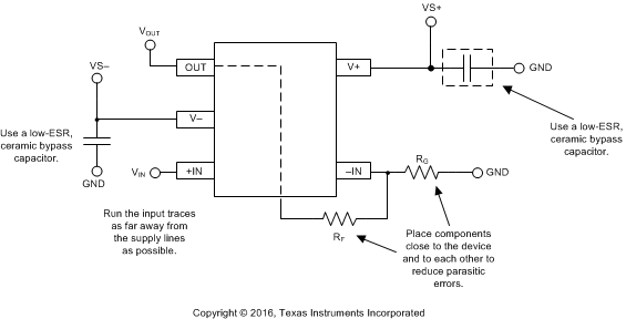
The OPA320 is a wideband amplifier. To realize the full operational performance of the device, good high-frequency PCB layout practices are required. The bypass capacitors must be connected between each supply pin and ground as close to the device as possible. The bypass capacitor traces should be designed for minimum inductance.

Layout Example

OPA320 OPA2320 OPA320S OPA2320S SOT_layout_example_SBOS538.gif Figure 49. Layout Example