SBOS522A June 2010 – November 2019 OPA333-Q1
PRODUCTION DATA.
- 1 Features
- 2 Applications
- 3 Description
- 4 Revision History
- 5 Pin Configuration and Functions
- 6 Specifications
- 7 Detailed Description
-
8 Application and Implementation
- 8.1 Application Information
- 8.2
Typical Applications
- 8.2.1 High-Side Voltage-to-Current (V-I) Converter
- 8.2.2 Precision, Low-Level Voltage-to-Current (V-I) Converter
- 8.2.3 Composite Amplifier
- 8.2.4 Temperature Measurement
- 8.2.5 Single Op-Amp Bridge-Amplifier
- 8.2.6 Low-Side Current-Monitor
- 8.2.7 High-Side Current Monitor
- 8.2.8 Thermistor Measurement
- 8.2.9 Precision Instrumentation Amplifier
- 9 Power Supply Recommendations
- 10Layout
- 11Device and Documentation Support
- 12Mechanical, Packaging, and Orderable Information
Package Options
Mechanical Data (Package|Pins)
- DBV|5
Thermal pad, mechanical data (Package|Pins)
Orderable Information
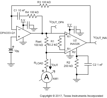
8.2.2 Precision, Low-Level Voltage-to-Current (V-I) Converter
The circuit shown in Figure 22 is a precision, low-level voltage-to-current (V-I) converter. The converter translates in input voltage of 0 V to 5 V and output current of 0 µA to 5 µA. Figure 23 shows the measured transfer function for this circuit. The low offset voltage and offset drift of the OPA333-Q1 facilitate excellent dc accuracy for the circuit. Figure 24 shows the calibrated error for the entire range of the circuit.
 Figure 22. Low-Level, Precision V-I Converter