SBOS235F March 2002 – April 2018 OPA2357 , OPA357
PRODUCTION DATA.
- 1 Features
- 2 Applications
- 3 Description
- 4 Revision History
- 5 Pin Configuration and Functions
- 6 Specifications
-
7 Detailed Description
- 7.1 Overview
- 7.2 Functional Block Diagram
- 7.3
Feature Description
- 7.3.1 OPAx357 Comparison
- 7.3.2 Operating Voltage
- 7.3.3 Enable Function
- 7.3.4 Rail-to-Rail Input
- 7.3.5 Rail-to-Rail Output
- 7.3.6 Output Drive
- 7.3.7 Video
- 7.3.8 Wideband Video Multiplexing
- 7.3.9 Driving Analog-to-Digital Converters
- 7.3.10 Capacitive Load and Stability
- 7.3.11 Wideband Transimpedance Amplifier
- 7.4 Device Functional Modes
- 8 Application and Implementation
- 9 Power Supply Recommendations
- 10Layout
- 11Device and Documentation Support
- 12Mechanical, Packaging, and Orderable Information
Package Options
Mechanical Data (Package|Pins)
- DBV|6
Thermal pad, mechanical data (Package|Pins)
Orderable Information
7.3.11 Wideband Transimpedance Amplifier
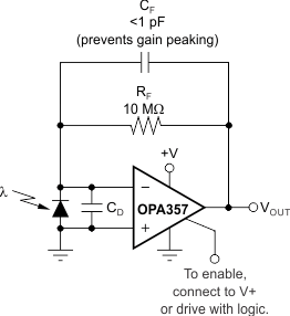
Wide bandwidth, low input bias current, and low input voltage and current noise make the OPA357 an ideal wideband photodiode transimpedance amplifier for low-voltage single-supply applications. Low-voltage noise is important because photodiode capacitance causes the effective noise gain of the circuit to increase at high frequency.
The key elements to a transimpedance design, as shown in Figure 40, are the expected diode capacitance (including the parasitic input common-mode and differential-mode input capacitance (2 + 2)pF for the OPA357), the desired transimpedance gain (RF), and the gain bandwidth product (GBP) for the OPA357 (100 MHz). With these three variables set, the feedback capacitor value (CF) can be set to control the frequency response.
 Figure 40. Transimpedance Amplifier
To achieve a maximally flat 2nd-order Butterworth frequency response, set the feedback pole to:

Typical surface-mount resistors have a parasitic capacitance of approximately 0.2 pF that must be deducted from the calculated feedback capacitance value.
Bandwidth is calculated by:

For even higher transimpedance bandwidth, the high-speed CMOS OPA355 (200-MHz GBW) or the OPA655 (400-MHz GBW) can be used.