SBOS279F September 2003 – September 2016 OPA2373 , OPA2374 , OPA373 , OPA374 , OPA4374
PRODUCTION DATA.
- 1 Features
- 2 Applications
- 3 Description
- 4 Revision History
- 5 Device Comparison Table
- 6 Pin Configuration and Functions
-
7 Specifications
- 7.1 Absolute Maximum Ratings
- 7.2 ESD Ratings
- 7.3 Recommended Operating Conditions
- 7.4 Thermal Information: OPA373
- 7.5 Thermal Information: OPA374
- 7.6 Thermal Information: OPA2373
- 7.7 Thermal Information: OPA2374
- 7.8 Thermal Information: OPA4374
- 7.9 Electrical Characteristics: VS = 2.7 V to 5.5 V
- 7.10 Typical Characteristics
- 8 Detailed Description
- 9 Application and Implementation
- 10Power Supply Recommendations
- 11Layout
- 12Device and Documentation Support
- 13Mechanical, Packaging, and Orderable Information
Package Options
Mechanical Data (Package|Pins)
Thermal pad, mechanical data (Package|Pins)
Orderable Information
8 Detailed Description
8.1 Overview
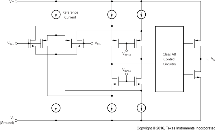
The OPAx373 and OPAx374 operational amplifiers (op amps) are suitable for a broad range of general-purpose applications. As unity-gain stable devices and outstanding AC performance, these op amps are ideal for audio applications. The class AB output stage is capable of driving 100-kΩ loads connected to any point between V+ and ground. These devices are well-suited for nearly any single-supply application up to a supply voltage of
5.5 V because the input common-mode voltage range includes both rails. Rail-to-rail input and output swing significantly increases the overall device dynamic range, especially in low-supply applications.
8.2 Functional Block Diagram
8.3 Feature Description
8.3.1 Operating Voltage
The OPA373 and OPA374 op amps are specified and tested over a power-supply range of 2.7 V to 5.5 V
(±1.35 V to ±2.75 V). However, the supply voltage may range from 2.3 V to 5.5 V (±1.15 V to ±2.75 V). Supply voltages higher than 7 V (absolute maximum) can permanently damage the amplifier. Parameters that vary over supply voltage or temperature are shown in the Typical Characteristics.
8.3.2 Common-Mode Voltage Range
The input common-mode voltage range of the OPA373 and OPA374 series extends 200 mV beyond the supply rails. This extended range is achieved with a complementary input stage: an N-channel input differential pair in parallel with a P-channel differential pair. The N-channel pair is active for input voltages close to the positive rail, typically (V+) − 1.65 V to 200 mV above the positive supply, while the P-channel pair is on for inputs from
200 mV below the negative supply to approximately (V+) − 1.65 V. There is a 500-mV transition region, typically (V+) − 1.9 V to (V+) − 1.4 V, in which both pairs are on. This 500-mV transition region, shown in Figure 21, can vary ±300 mV with process variation. Thus, the transition region (that is, both stages on) can range from
(V+) − 2.2 V to (V+) − 1.7 V on the low end, up to (V+) − 1.6 V to (V+) − 1.1 V on the high end. Within the
500-mV transition region, PSRR, CMRR, offset voltage, offset drift, and THD may be degraded, compared to device operation outside this region.
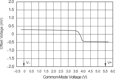 Figure 21. Behavior of Typical Transition Region at Room Temperature
8.3.3 Rail-to-Rail Input
The input common-mode range extends from (V−) − 0.2 V to (V+) + 0.2 V. For normal operation, inputs must be limited to this range. The absolute maximum input voltage is 500 mV beyond the supplies. Inputs greater than the input common-mode range but less than the maximum input voltage, while not valid, do not cause any damage to the op amp. Unlike some other op amps, if input current is limited, the inputs may go beyond the supplies without phase inversion, as shown in Figure 22.
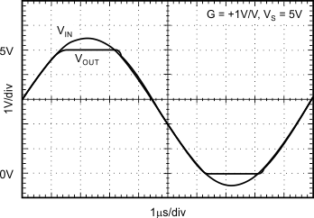 Figure 22. OPA373: No Phase Inversion With Inputs Greater Than the Power-Supply Voltage
Normally, input bias current is approximately 500 fA; however, input voltages exceeding the power supplies by more than 500 mV can cause excessive current to flow in or out of the input pins. Momentary voltages greater than 500 mV beyond the power supply can be tolerated if the current on the input pins is limited to 10 mA. This limiting is easily accomplished with an input resistor; see Figure 23. Many input signals are inherently current-limited to less than 10 mA, therefore, a limiting resistor is not required.
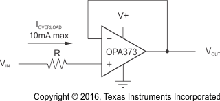 Figure 23. Input Current Protection for Voltages Exceeding the Supply Voltage
8.3.4 Rail-to-Rail Output
A class AB output stage with common-source transistors is used to achieve rail-to-rail output. For light resistive loads ( > 100 kΩ), the output voltage can typically swing to within 18 mV from the supply rails. With moderate resistive loads (5 kΩ to 50 kΩ), the output can typically swing to within 100 mV from the supply rails and maintain high open-loop gain. See Figure 12 for more information.
8.3.5 Capacitive Load and Stability
The OPA373 series op amps can drive a wide range of capacitive loads. However, under certain conditions, all op amps may become unstable. Op amp configuration, gain, and load value are some of the factors to consider when determining stability. An op amp in unity-gain configuration is the most susceptible to the effects of capacitive load. The capacitive load reacts with the op amp output resistance, along with any additional load resistance, to create a pole in the small-signal response that degrades the phase margin. The OPA373 series op amps perform well in unity-gain configuration, with a pure capacitive load up to approximately 250 pF. Increased gains allow the amplifier to drive more capacitance. See Figure 17 for further details.
One method of improving capacitive load drive in the unity-gain configuration is to insert a small (10-Ω to 20-Ω) resistor, RS, in series with the output, as shown in Figure 24. This configuration significantly reduces ringing while maintaining DC performance for purely capacitive loads. When there is a resistive load in parallel with the capacitive load, RS must be placed within the feedback loop as shown to allow the feedback loop to compensate for the voltage divider created by RS and RL.
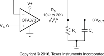 Figure 24. Series Resistor in Unity-Gain Configuration Improves Capacitive Load Drive
In unity-gain inverter configuration, phase margin can be reduced by the reaction between the capacitance at the op amp input and the gain setting resistors, thus degrading capacitive load drive. Best performance is achieved by using small-valued resistors. However, when large-valued resistors cannot be avoided, a small (4-pF to 6-pF) capacitor, CFB, can be inserted in the feedback, as shown in Figure 25. This technique significantly reduces overshoot by compensating the effect of capacitance, CIN, which includes the amplifier input capacitance and printed-circuit board (PCB) parasitic capacitance.
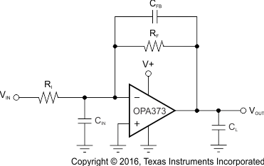 Figure 25. Improving Capacitive Load Drive
For example, when driving a 100-pF load in unity-gain inverter configuration, adding a 6-pF capacitor in parallel with the 10-kΩ feedback resistor decreases overshoot from 57% to 12%, as shown in Figure 26.
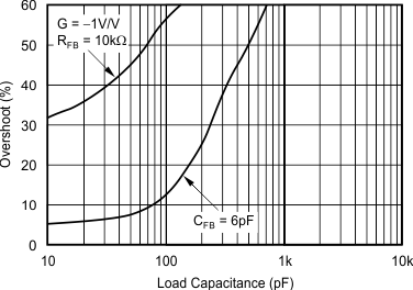 Figure 26. Improving Capacitive Load Drive
8.3.6 Enable or Shutdown
The OPA373 and OPA374 series op amps typically require 585-µA quiescent current. The enable or shutdown feature of the OPA373 allows the op amp to be shut off to reduce this current to less than 1 µA.
8.4 Device Functional Modes
The OPAx374 has a single functional mode and is operational when the power-supply voltage is greater than
2.7 V (±1.35 V). The maximum power supply voltage for the OPAx374 is 5.5 V (±2.75 V).
The OPAx373 has two functional modes: active and shutdown. When the voltage at the Enable pin is from V– to (V–) + 0.8 V, the device is in shutdown and consumes less than 0.5 µA of quiescent current (typical). To activate, or enable, the device, the voltage at the Enable pin must be from (V–) + 2 V to V+. When active, the power-supply requirements are the same as the OPAx374.