SBOSA02 August 2021 OPA397
PRODUCTION DATA
- 1 Features
- 2 Applications
- 3 Description
- 4 Revision History
- 5 Pin Configuration and Functions
- 6 Specifications
- 7 Detailed Description
- 8 Application and Implementation
- 9 Power Supply Recommendations
- 10Layout
- 11Device and Documentation Support
- 12Mechanical, Packaging, and Orderable Information
Package Options
Mechanical Data (Package|Pins)
- DBV|5
Thermal pad, mechanical data (Package|Pins)
Orderable Information
5 Pin Configuration and Functions
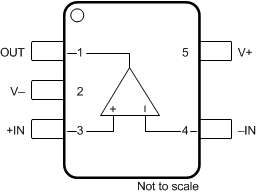
 Figure 5-1 OPA397 DCK Package (5-Pin SOT, Preview), Top View
Figure 5-3 OPA397 YCJ Package (6-Pin DSBGA, Preview), Top View
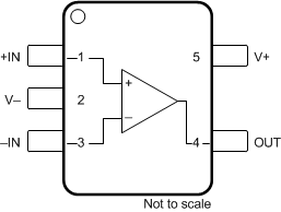
 Figure 5-2 OPA397 DBV Package (5-Pin SOT-23), Top View
Table 5-1 Pin Functions: OPA397
| PIN | I/O | DESCRIPTION | |||
|---|---|---|---|---|---|
| NAME | NO. | ||||
| DBV (SOT-23) | DCK (SC-70) | YCJ (DSBGA) | |||
| –IN | 4 | 3 | B1 | I | Inverting input |
| +IN | 3 | 1 | A1 | I | Noninverting input |
| EN | — | — | B2 | I | Enable pin. High = amplifier enabled. |
| OUT | 1 | 4 | C1 | O | Output |
| V– | 2 | 2 | A2 | — | Negative (lowest) power supply |
| V+ | 5 | 5 | C2 | — | Positive (highest) power supply |
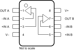
 Figure 5-4 OPA2397 D (8-Pin SOIC, Preview) and DGK (8-Pin MSOP, Preview)
Packages, Top View
Figure 5-4 OPA2397 D (8-Pin SOIC, Preview) and DGK (8-Pin MSOP, Preview)
Packages, Top ViewFigure 5-5 OPA2397 YBJ (9-Pin DSBGA, Preview) Package, Top View
Table 5-2 Pin Functions: OPA2397
| PIN | I/O | DESCRIPTION | ||
|---|---|---|---|---|
| NAME | NO. | |||
| D (SOIC), DGK (VSSOP) |
YBJ (DSBGA) | |||
| –IN A | 2 | B3 | I | Inverting input, channel A |
| –IN B | 6 | B1 | I | Inverting input, channel B |
| +IN A | 3 | A3 | I | Noninverting input, channel A |
| +IN B | 5 | A1 | I | Noninverting input, channel B |
| EN | — | B2 | I | Enable pin. High = both amplifiers enabled. |
| OUT A | 1 | C3 | O | Output, channel A |
| OUT B | 7 | C1 | O | Output, channel B |
| V– | 4 | A2 | — | Negative (lowest) power supply |
| V+ | 8 | C2 | — | Positive (highest) power supply |
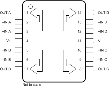
 Figure 5-6 OPA4397 PW (14-Pin TSSOP, Preview) Package, Top View
Figure 5-7 OPA4397 RTE (16-Pin QFN, Preview) Package, Top View
Table 5-3 Pin Functions: OPA4397
| PIN | I/O | DESCRIPTION | ||
|---|---|---|---|---|
| NAME | NO. | |||
| PW (TSSOP) | RTE (QFN) | |||
| –IN A | 2 | 16 | I | Inverting input, channel A |
| –IN B | 6 | 4 | I | Inverting input, channel B |
| –IN C | 9 | 9 | I | Inverting input, channel C |
| –IN D | 13 | 13 | I | Inverting input, channel D |
| +IN A | 3 | 1 | I | Noninverting input, channel A |
| +IN B | 5 | 3 | I | Noninverting input, channel B |
| +IN C | 10 | 10 | I | Noninverting input, channel C |
| +IN D | 12 | 12 | I | Noninverting input, channel D |
| EN AB | — | 6 | I | Enable pin for A and B amplifiers. High = amplifiers A and B are enabled. |
| EN CD | — | 7 | I | Enable pin for C and D amplifiers. High = amplifiers C and D are enabled. |
| OUT A | 1 | 15 | O | Output, channel A |
| OUT B | 7 | 5 | O | Output, channel B |
| OUT C | 8 | 8 | O | Output, channel C |
| OUT D | 14 | 14 | O | Output, channel D |
| Thermal Pad | — | Thermal Pad | — | Connect thermal pad to V– |
| V– | 11 | 11 | — | Negative (lowest) power supply |
| V+ | 4 | 2 | — | Positive (highest) power supply |