SBOS641D June 2012 – September 2016 OPA4188
PRODUCTION DATA.
- 1 Features
- 2 Applications
- 3 Description
- 4 Revision History
- 5 Zero-Drift Amplifier Portfolio
- 6 Pin Configuration and Functions
-
7 Specifications
- 7.1 Absolute Maximum Ratings
- 7.2 ESD Ratings
- 7.3 Recommended Operating Conditions
- 7.4 Thermal Information
- 7.5 Electrical Characteristics: High-Voltage Operation, VS = ±4 V to ±18 V (VS = 8 V to 36 V)
- 7.6 Electrical Characteristics: Low-Voltage Operation, VS = ±2 V to < ±4 V (VS = +4 V to < +8 V)
- 7.7 Typical Characteristics
- 8 Detailed Description
- 9 Applications and Implementation
- 10Power Supply Recommendations
- 11Layout
- 12Device and Documentation Support
- 13Mechanical, Packaging, and Orderable Information
Package Options
Mechanical Data (Package|Pins)
Thermal pad, mechanical data (Package|Pins)
Orderable Information
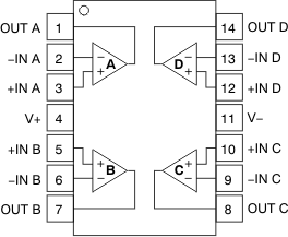
6 Pin Configuration and Functions
D or PW Packages
14-Pin SOIC or 14-Pin TSSOP
Top View

Pin Functions
| PIN | I/O | DESCRIPTION | |
|---|---|---|---|
| NO. | NAME | ||
| 1 | OUT A | O | Output channel A |
| 2 | –IN A | I | Inverting input channel A |
| 3 | +IN A | I | Noninverting input channel A |
| 4 | V+ | I | Positive power supply |
| 5 | +IN B | I | Noninverting input channel B |
| 6 | –IN B | I | Inverting input channel B |
| 7 | OUT B | O | Output channel B |
| 8 | OUT C | O | Output channel C |
| 9 | –IN C | I | Inverting input channel C |
| 10 | +IN C | I | Noninverting input channel C |
| 11 | V– | I | Negative power supply |
| 12 | +IN D | I | Noninverting input channel D |
| 13 | –IN D | I | Inverting input channel D |
| 14 | OUT D | O | Output channel D |