SLOS856B June 2013 – May 2017 OPA2322-Q1 , OPA322-Q1 , OPA4322-Q1
PRODUCTION DATA.
- 1 Features
- 2 Applications
- 3 Description
- 4 Revision History
- 5 Pin Configuration and Functions
- 6 Specifications
- 7 Typical Characteristics
- 8 Detailed Description
- 9 Application and Implementation
- 10Power Supply Recommendations
- 11Layout
- 12Device and Documentation Support
- 13Mechanical, Packaging, and Orderable Information
Package Options
Mechanical Data (Package|Pins)
- PW|14
Thermal pad, mechanical data (Package|Pins)
Orderable Information
8 Detailed Description
8.1 Overview
The OPAx322-Q1 family of operational amplifiers (op amps) are high-speed precision amplifiers well-suited to drive 12-, 14-, and 16-bit analog-to-digital converters. Low-output impedance with flat frequency characteristics and zero-crossover distortion circuitry enable high linearity over the full input common-mode range, achieving true rail-to-rail input from a 1.8-V to 5.5-V single-supply.
8.2 Functional Block Diagram
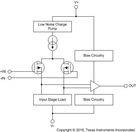
8.3 Feature Description
8.3.1 Operating Voltage
The OPAx322-Q1 series op amps are unity-gain stable and can operate on a single-supply voltage (1.8 V to 5.5 V), or a split-supply voltage (±0.9 V to ±2.75 V), which makes the op amps highly versatile and easy to use. The power-supply pins must have local bypass ceramic capacitors (typically 0.001 μF to 0.1 μF). These amplifiers are fully specified from 1.8 V to 5.5 V and over the extended temperature range from –40°C to +125°C. Parameters that can exhibit variance with regard to operating voltage or temperature are presented in Typical Characteristics.
8.3.2 Input and ESD Protection
The OPAx322-Q1 incorporates internal electrostatic discharge (ESD) protection circuits on all pins. In the case of input and output pins, this protection primarily consists of current-steering diodes connected between the input and power-supply pins. These ESD protection diodes also provide in-circuit input overdrive protection, as long as the current is limited to 10 mA as stated in Absolute Maximum Ratings. Many input signals are inherently current-limited to less than 10 mA; therefore, a limiting resistor is not required. Figure 26 shows how a series input resistor (RS) may be added to the driven input to limit the input current. The added resistor contributes thermal noise at the amplifier input and the value must be kept to the minimum in noise-sensitive applications.
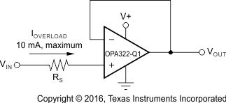 Figure 26. Input Current Protection
8.3.3 Phase Reversal
The OPAx322-Q1 family of op amps are designed to be immune to phase reversal when the input pins exceed the supply voltages, which provides further in-system stability and predictability. Figure 27 shows the input voltage exceeding the supply voltage without any phase reversal.
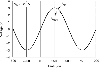 Figure 27. No Phase Reversal
8.3.4 Feedback Capacitor Improves Response
For optimum settling time and stability with high-impedance feedback networks, it may be necessary to add a feedback capacitor across the feedback resistor (RF), as shown in Figure 28. This capacitor compensates for the zero created by the feedback network impedance and the OPAx322-Q1 input capacitance (and any parasitic layout capacitance). The effect becomes more significant with higher impedance networks.
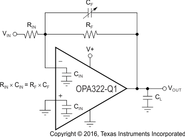
NOINDENT:
NOTE: Where CIN is equal to the OPAx322-Q1 input capacitance (approximately 9 pF) plus any parasitic layout capacitance.For the circuit shown in Figure 28, the value of the variable feedback capacitor must be selected so that the input resistance times the input capacitance of the OPAx322-Q1 (typically 9 pF) plus the estimated parasitic layout capacitance equals the feedback capacitor times the feedback resistor with Equation 1.
where
- CIN is equal to the OPAx322-Q1 input capacitance (sum of differential and common-mode) plus the layout capacitance
The capacitor value can be adjusted until optimum performance is obtained.
8.3.5 EMI Susceptibility and Input Filtering
Operational amplifiers vary in susceptibility to electromagnetic interference (EMI). If conducted EMI enters the device, the DC offset observed at the amplifier output may shift from the nominal value while EMI is present. This shift is a result of signal rectification associated with the internal semiconductor junctions. While all operational amplifier pin functions can be affected by EMI, the input pins are likely to be the most susceptible. The OPAx322-Q1 operational amplifier family incorporates an internal input low-pass filter that reduces the amplifier response to EMI. Both common-mode and differential mode filtering are provided by the input filter. The filter is designed for a cutoff frequency of approximately 580 MHz (–3 dB), with a roll-off of 20 dB per decade.
8.3.6 Output Impedance
The open-loop output impedance of the OPAx322-Q1 common-source output stage is approximately 90 Ω. When the op amp is connected with feedback, the loop gain significantly reduces this value. For each decade rise in the closed-loop gain, the loop gain is reduced by the same amount, which results in a tenfold increase in effective output impedance. While the OPAx322-Q1 output impedance remains flat over a wide frequency range. At higher frequencies the output impedance rises as the open-loop gain of the op amp drops. However, at these frequencies the output becomes capacitive as a result of parasitic capacitance. This characteristic prevents the output impedance from becoming too high, which can cause stability problems when driving large capacitive loads. As mentioned previously, the OPAx322-Q1 has excellent capacitive load drive capability for an op amp with a bandwidth of this value.
8.3.7 Capacitive Load and Stability
The OPAx322-Q1 is designed to be used in applications where driving a capacitive load is required. As with all op amps, there may be specific instances where the OPAx322-Q1 can become unstable. The particular op amp circuit configuration, layout, gain, and output loading are some of the factors to consider when establishing whether an amplifier is stable in operation. An op amp in the unity-gain (1-V/V) buffer configuration and driving a capacitive load exhibits a greater tendency to become unstable than an amplifier operating at a higher noise gain. The capacitive load, in conjunction with the op amp output resistance, creates a pole within the feedback loop that degrades the phase margin.
The equivalent series resistance (ESR) of some very large capacitors (CL > 1 µF) is sufficient to alter the phase characteristics in the feedback loop so the amplifier remains stable. Increasing the amplifier closed-loop gain allows the amplifier to drive increasingly larger capacitance. This increased capability is evident when observing the overshoot response of the amplifier at higher voltage gains, as shown in Figure 29. One technique for increasing the capacitive load drive capability of the amplifier operating in unity gain is to insert a small resistor (RS, typically 10-Ω to 20-Ω) in series with the output, as shown in Figure 30.
This resistor significantly reduces the overshoot and ringing associated with large capacitive loads. A possible problem with this technique is that a voltage divider is created with the added series resistor and any resistor connected in parallel with the capacitive load. The voltage divider introduces a gain error at the output that reduces the output swing. However, the error contributed by the voltage divider may be insignificant. For example, with a load resistance of RL = 10 kΩ and RS = 20 Ω, the gain error is approximately 0.2%. When RL decreases to 600 Ω (which the OPAx322-Q1 is able to drive), the error increases to 7.5%.
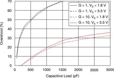 Figure 29. Small-Signal Overshoot vs Capacitive Load (100-mVPP Output Step)
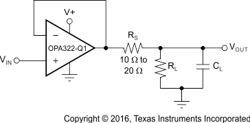 Figure 30. Improving Capacitive Load Drive
8.3.8 Overload Recovery Time
Overload recovery time is the time required for the output of the amplifier to come out of saturation and recover to the linear region. Overload recovery is particularly important in applications where small signals must be amplified in the presence of large transients. Figure 31 and Figure 32 show the positive and negative overload recovery times of the OPAx322-Q1, respectively. In both cases, the time elapsed before the OPAx322-Q1 comes out of saturation is less than 100 ns. The symmetry between the positive and negative recovery times allows excellent signal rectification without distortion of the output signal.
spacer
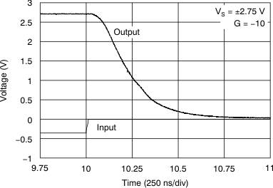 Figure 31. Positive Recovery Time
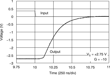 Figure 32. Negative Recovery Time