SBOS984G November 2020 – September 2023 OPA2387 , OPA387 , OPA4387
PRODUCTION DATA
- 1
- 1 Features
- 2 Applications
- 3 Description
- 4 Revision History
- 5 Pin Configuration and Functions
- 6 Specifications
- 7 Detailed Description
- 8 Application and Implementation
- 9 Device and Documentation Support
- 10Mechanical, Packaging, and Orderable Information
Package Options
Mechanical Data (Package|Pins)
- PW|14
Thermal pad, mechanical data (Package|Pins)
Orderable Information
8.2.1.2 Detailed Design Procedure
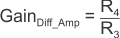
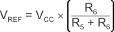
The load current, ILOAD, flows through the shunt resistor, RSHUNT, to develop the shunt voltage, VSHUNT. The shunt voltage is then amplified by the difference amplifier consisting of U1A and R1 through R4. The gain of the difference amplifier is set by the ratio of R4 to R3. To minimize errors, set R2 = R4 and R1 = R3. The reference voltage, VREF, is supplied by buffering a resistor divider using U1B. The transfer function is given by Equation 1.

where

There are two types of errors in this design: gain and offset. Gain errors are introduced by the tolerance of the shunt resistor and the ratios of R4 to R3 and, similarly, R2 to R1. Offset errors are introduced by the voltage divider (R5 and R6) and how closely the ratio of R4 / R3 matches R2 / R1. The latter value affects the CMRR of the difference amplifier, ultimately translating to an offset error.
The value of VSHUNT is the ground potential for the system load because VSHUNT is a low-side measurement. Therefore, a maximum value must be placed on VSHUNT. In this design, the maximum value for VSHUNT is set to 100 mV. Equation 2 calculates the maximum value of the shunt resistor given a maximum shunt voltage of 100 mV and maximum load current of 1 A.
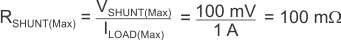
The tolerance of RSHUNT is directly proportional to cost. For this design, a shunt resistor with a tolerance of 0.5% is selected. If greater accuracy is required, select a 0.1% resistor or better.
The load current is bidirectional; therefore, the shunt voltage range is –100 mV to +100 mV. This voltage is divided down by R1 and R2 before reaching the operational amplifier, U1A. Make sure that the voltage present at the noninverting node of U1A is within the common-mode range of the device. Use an operational amplifier, such as the OPAx387, that has a common-mode range that extends below the negative supply voltage. The offset error is minimal because the OPAx387 has a typical offset voltage of merely ±0.25 µV (±5 µV, maximum).
Given a symmetric load current of –1 A to +1 A, the voltage divider resistors, R5 and R6, must be equal. To be consistent with the shunt resistor, a tolerance of 0.5% is selected. To minimize power consumption, 10‑kΩ resistors are used.
To set the gain of the difference amplifier, the common-mode range and output swing of the OPAx387 must be considered. Equation 3 and Equation 4 depict the typical common-mode range and maximum output swing, respectively, of the OPAx387 given a 3.3‑V supply.
The gain of the difference amplifier can now be calculated as shown in Equation 5.

The resistor value selected for R1 and R3 is 1 kΩ. 15.4 kΩ is selected for R2 and R4 because this number is the nearest standard value. Therefore, the ideal gain of the difference amplifier is 15.4 V/V.
The gain error of the circuit primarily depends on R1 through R4. As a result of this dependence, 0.1% resistors were selected. This configuration reduces the likelihood that the design requires a two-point calibration. A simple one-point calibration, if desired, removes the offset errors introduced by the 0.5% resistors.