SBOS391B December 2007 – March 2016 OPA454
PRODUCTION DATA.
- 1 Features
- 2 Applications
- 3 Description
- 4 Revision History
- 5 Device Comparison Table
- 6 Pin Configuration and Functions
- 7 Specifications
- 8 Parameter Measurement Information
- 9 Detailed Description
- 10Application and Implementation
- 11Power Supply Recommendations
- 12Layout
- 13Device and Documentation Support
- 14Mechanical, Packaging, and Orderable Information
Package Options
Mechanical Data (Package|Pins)
- DDA|8
Thermal pad, mechanical data (Package|Pins)
- DDA|8
Orderable Information
7 Specifications
7.1 Absolute Maximum Ratings
over operating free-air temperature range (unless otherwise noted)(1)| MIN | MAX | UNIT | ||
|---|---|---|---|---|
| Voltage | Supply voltage, VS = (V+) – (V–) | 120 | V | |
| Signal input pin(2) | (V–) – 0.3 | (V+) + 0.3 | V | |
| E/D to E/D Com | 5.5 | V | ||
| Current | Signal input pin(2) | ±10 | mA | |
| Output short circuit(3) | Continuous | |||
| Temperature | Operating, TA | –55 | 125 | °C |
| Junction, TJ | 150 | °C | ||
| Storage, Tstg | –55 | 125 | °C | |
(1) Stresses beyond those listed under Absolute Maximum Ratings may cause permanent damage to the device. These are stress ratings only, which do not imply functional operation of the device at these or any other conditions beyond those indicated under Recommended Operating Conditions. Exposure to absolute-maximum-rated conditions for extended periods may affect device reliability.
(2) Input terminals are diode-clamped to the power-supply rails. Input signals that can swing more than 0.3 V beyond the supply rails must be current-limited to 10 mA or less.
(3) Short-circuit to ground.
7.2 ESD Ratings
| VALUE | UNIT | |||
|---|---|---|---|---|
| V(ESD) | Electrostatic discharge | Human-body model (HBM), per ANSI/ESDA/JEDEC JS-001(1) | ±4000 | V |
| Charged-device model (CDM), per JEDEC specification JESD22-C101(2) | ±500 | |||
| Machine model (MM) | ±150 | |||
(1) JEDEC document JEP155 states that 500-V HBM allows safe manufacturing with a standard ESD control process.
(2) JEDEC document JEP157 states that 250-V CDM allows safe manufacturing with a standard ESD control process.
7.3 Recommended Operating Conditions
over operating free-air temperature range (unless otherwise noted)| MIN | NOM | MAX | UNIT | ||
|---|---|---|---|---|---|
| Supply voltage, VS = (V+) – (V–) | 10 (±5) | 100 (±50) | V | ||
| TA | Operating temperature | –55 | 125 | °C | |
7.4 Thermal Information
| THERMAL METRIC(1) | OPA454 | UNIT | |
|---|---|---|---|
| DDA (SO) | |||
| 8 PINS | |||
| RθJA | Junction-to-ambient thermal resistance | 40.6 | °C/W |
| RθJC(top) | Junction-to-case (top) thermal resistance | 46 | °C/W |
| RθJB | Junction-to-board thermal resistance | 20.7 | °C/W |
| ψJT | Junction-to-top characterization parameter | 5.6 | °C/W |
| ψJB | Junction-to-board characterization parameter | 20.6 | °C/W |
| RθJC(bot) | Junction-to-case (bottom) thermal resistance | 2.5 | °C/W |
(1) For more information about traditional and new thermal metrics, see the Semiconductor and IC Package Thermal Metrics application report, SPRA953.
7.5 Electrical Characteristics: VS = ±50 V
At TP(1) = 25°C, RL = 4.8 kΩ to mid-supply, VCM = VOUT = mid-supply, unless otherwise noted.| PARAMETER | TEST CONDITIONS | MIN | TYP | MAX | UNIT | ||
|---|---|---|---|---|---|---|---|
| OFFSET VOLTAGE | |||||||
| VOS | Input offset voltage | IO = 0 mA | ±0.2 | ±4 | mV | ||
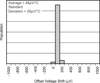
| dVOS/dT | Input offset voltage vs temperature | At TA = –40°C to +85°C | ±1.6 | ±10 | µV/°C | ||
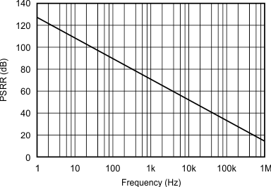
| PSRR | Input offset voltage vs power supply | VS = ±4 V to ±60 V, VCM = 0 V | 25 | 100 | µV/V | ||
| INPUT BIAS CURRENT | |||||||
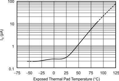
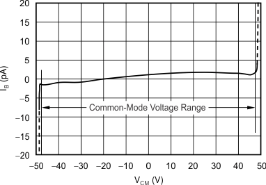
| IB | Input bias current | At TP = 25°C | ±1.4 | ±100 | pA | ||
| At TA = –40°C to +85°C | See Typical Characteristics | ||||||
| IOS | Input offset current | ±0.2 | ±100 | pA | |||
| NOISE | |||||||
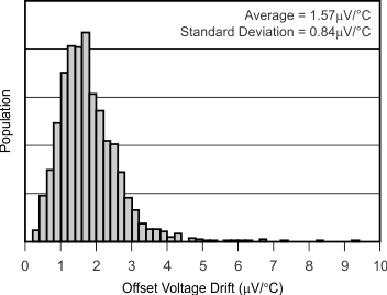
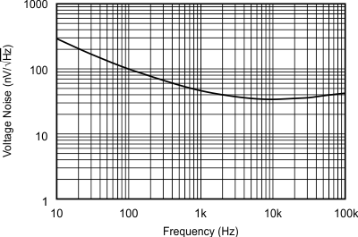
| en | Input voltage noise density | f = 10 Hz | 300 | nV/√Hz | |||
| f = 10 kHz | 35 | nV/√Hz | |||||
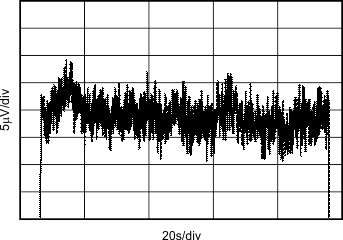
| Input voltage noise | f = 0.01 Hz to 10 Hz | 15 | µVPP | ||||
| in | Current noise density | f = 1 kHz | 40 | fA/√Hz | |||
| INPUT VOLTAGE RANGE | |||||||
| VCM | Common-mode voltage range | Linear operation | (V–) + 2.5 | See Note (12) | (V+) – 2.5 | V | |
| CMRR | Common-mode rejection | VS = ±50 V, –25 V ≤ VCM ≤ 25 V | 100 | 146 | dB | ||
| VS = ±50 V, –45 V ≤ VCM ≤ 45 V | 100 | 147 | dB | ||||
| At TA = –40°C to +85°C, VS = ±50 V, –25 V ≤ VCM ≤ 25 V |
80 | 88 | dB | ||||
| At TA = –40°C to +85°C, VS = ±50 V, –45 V ≤ VCM ≤ 45 V |
72 | 82 | dB | ||||
| INPUT IMPEDANCE | |||||||
| Differential | 1013 || 10 | Ω || pF | |||||
| Common-mode | 1013 || 9 | Ω || pF | |||||
| OPEN-LOOP GAIN | |||||||
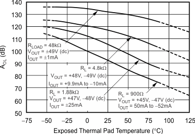
| AOL | Open-loop voltage gain(2) |
(V–) + 1 V < VO < (V+) – 1 V, RL = 49 kΩ, IO = ±1 mA |
100 | 130 | dB | ||
| At TA = –40°C to +85°C | 112 | dB | |||||
| (V–) + 1 V < VO < (V+) – 2 V, RL = 4.8 kΩ, IO = ±10 mA |
100 | 115 | dB | ||||
| At TA = –40°C to +85°C | 106 | dB | |||||
| (V–) + 2 V < VO < (V+) – 3 V, RL = 1880 Ω, IO = ±25 mA |
80 | 102 | dB | ||||
| At TA = –40°C to +85°C | 84 | dB | |||||
| FREQUENCY RESPONSE(3) | |||||||
| GBW | Gain-bandwidth product | Small-signal | 2.5 | MHz | |||
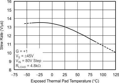
| SR | Slew rate | G = ±1, VO = 80-V step, RL = 3.27 kΩ |
13 | V/µs | |||
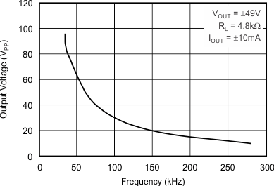
| Full-power bandwidth(4) | 35 | kHz | |||||
| tS | Settling time(5) | To ±0.1%, G = ±1, VO = 20-V step | 3 | µs | |||
| To ±0.01%, G = ±5 or ±10, VO = 80-V step |
10 | µs | |||||
| THD+N | Total harmonic distortion + noise(6) | VS = +40.6 V/–39.6 V, G = ±1, f = 1 kHz, VO = 77.2 VPP |
0.0008% | ||||
| OUTPUT | |||||||
| VO | Voltage output swing from rail(7) | RL = 49 kΩ, AOL ≥ 100 dB, IO = 1 mA |
(V–) + 1 | (V+) – 1 | V | ||
| RL = 4.8 kΩ, AOL ≥ 100 dB, IO = 10 mA |
(V–) + 1 | (V+) – 2 | V | ||||
| RL = 1880 Ω, AOL ≥ 80 dB, IO = 26 mA |
(V–) + 2 | (V+) – 3 | V | ||||
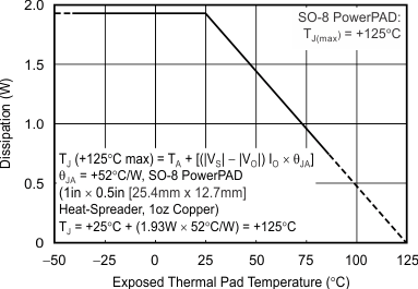
| Continuous current output, DC | Depends on circuit conditions | See Figure 5 | |||||
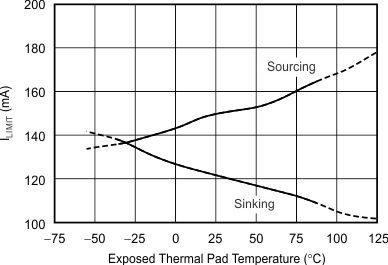
| IO | Maximum peak current output, current limit(2) | +120/–150 | mA | ||||
| At TA = –40°C to +85°C | +140/–170 | mA | |||||
| CLOAD | Capacitive load drive(3) | 200 | pF | ||||
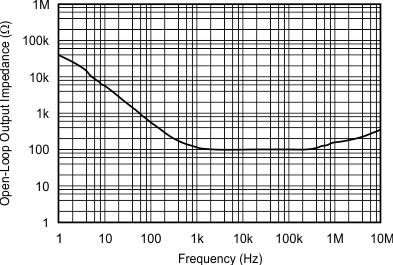
| RO | Open-loop output impedance | See Figure 4 | Ω | ||||
| Output disabled | Output capacitance | 18 | pF | ||||
| Feedthrough capacitance(8) | 150 | fF | |||||
| STATUS FLAG PIN (Referenced to E/D Com) | |||||||
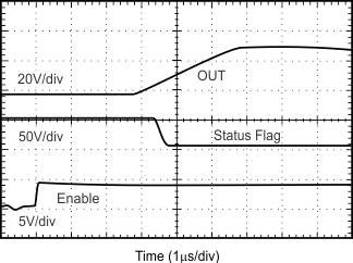
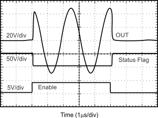
| Status Flag delay | Enable → Disable | 6 | µs | ||||
| Disable → Enable | 4 | µs | |||||
| Overcurrent delay(10) | 15 | µs | |||||
| Overcurrent recovery delay(10) | 10 | µs | |||||
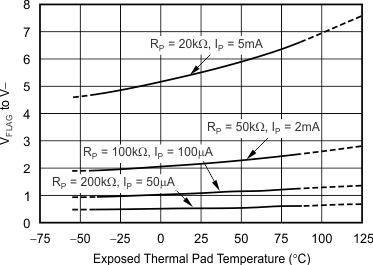
| TJ | Junction temperature | Alarm (Status Flag high) | 150 | °C | |||
| Return to normal operation (Status Flag low) |
130 | °C | |||||
| Output voltage(3) | Normal operation | E/D Com + 2 | V | ||||
| RL = 100 Ω during thermal overdrive, alarm | (V+) – 2.5 | V | |||||
| E/D (ENABLE/DISABLE) PIN | |||||||
| E/D pin, referenced to E/D Com pin(11)(9) | |||||||
| VSD | High (output enabled) | Pin open or forced high | E/D Com + 2.5 | E/D Com + 5 | V | ||
| Low (output disabled) | Pin forced low | E/D Com | E/D Com + 0.65 | V | |||
| Output disable time | 4 | µs | |||||
| Output enable time | 3 | µs | |||||
| E/D COM PIN | |||||||
| Voltage range | (V–) | (V+) – 5 | V | ||||
| POWER SUPPLY | |||||||
| VS | Specified range | ±50 | V | ||||
| Operating voltage range | ±5 | ±50 | V | ||||
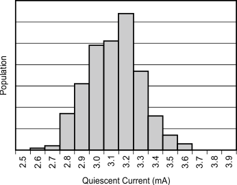
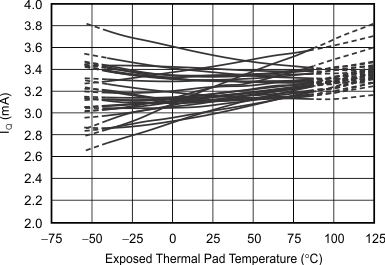
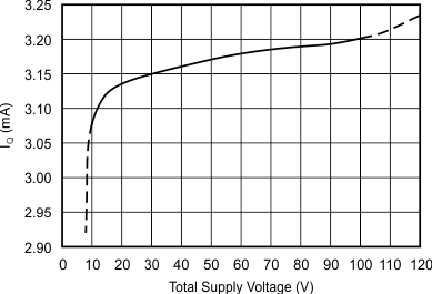
| IQ | Quiescent current | IO = 0 mA | 3.2 | 4 | mA | ||
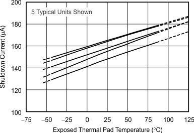
| Quiescent current in Shutdown mode | IO = 0 mA, VE/D = 0.65 V | 150 | 210 | µA | |||
| TEMPERATURE RANGE | |||||||
| TA | Specified range | –40 | 85 | °C | |||
| Operating range | –55 | 125 | °C | ||||
(1) TP is the temperature of the leadframe die pad (exposed thermal pad) of the PowerPAD package.
(2) Measured using low-frequency (<10 Hz) ±49-V square wave. See typical characteristic curve, Current Limit vs Temperature (Figure 23).
(3) See Typical Characteristics curves.
(4) See typical characteristic curve, Maximum Output Voltage vs Frequency (Figure 11).
(5) See the Feature Description section, Settling Time.
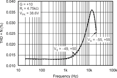
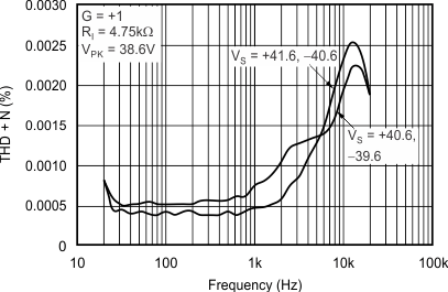
(6) Supplies reduced to allow closer swing to rails due to test equipment limitations. See typical characteristic curves Total Harmonic Distortion + Noise vs Frequency (Figure 29 and Figure 30) for additional power levels.
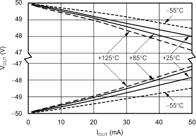
(7) See typical characteristic curve, Output Voltage Swing vs Output Current (Figure 10).
(8) Measured using Figure 56.
(9) High enables the outputs.
(10) See Typical Characteristics curves for current limit behavior.
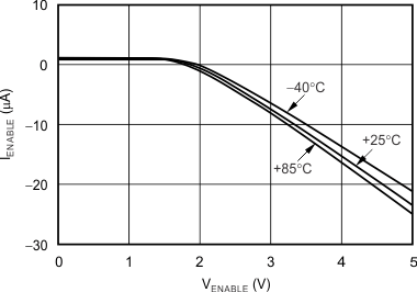
(11) See typical characteristic curve, IENABLE vs VENABLE (Figure 45).
(12) Typical range is (V–) + 1.5 V to (V+) – 1.5 V.
7.6 Typical Characteristics
At TP = 25°C, VS = ±50 V, and RL = 4.8 kΩ connected to GND, unless otherwise noted.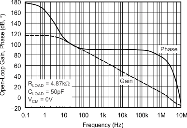
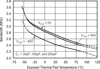
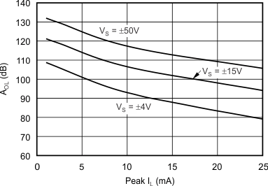
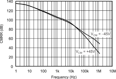
Temperature With Minimum Attach Area
| G = +2 | RF = 10 kΩ | VCM = 0 V |
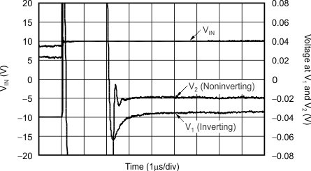
| See the Settling Time section. The grid for voltage at V1 and V2 is scaled 20 mV or 0.1% per division. | ||
| 20-V Step | Gain = 1 | RF = 10 kΩ |
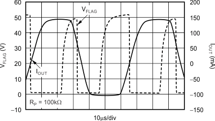
| The OPA454 was connected to sufficient heatsinking to prevent thermal shutdown. | ||
| TP = 125°C | ||
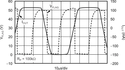
| The OPA454 was connected to sufficient heatsinking to prevent thermal shutdown. | ||
| TP = –55°C | ||
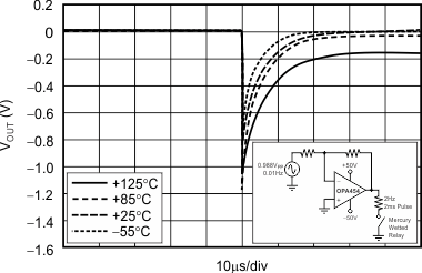
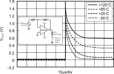
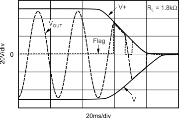
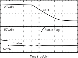
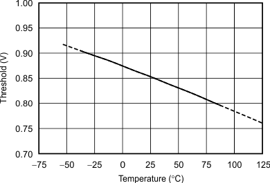
(Measured When Status Flag Transitions From
Low To High)
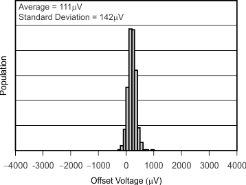
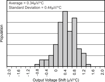
Production Distribution
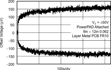
(60 Devices)
| See Figure 72 in the System Examples section. |
(E/D Com Connected To V–)
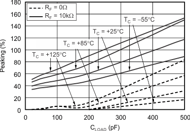
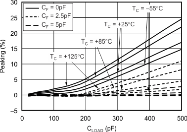
See Application section, Unity-Gain Noninverting Configuration.
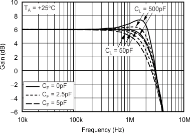
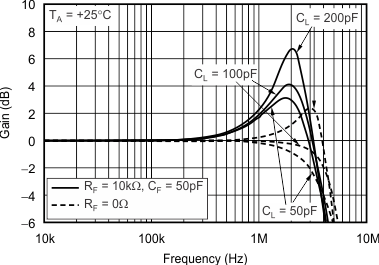
Figure 36. Gain Peaking vs CLOAD
| G = +1 | VCM = 0 V |
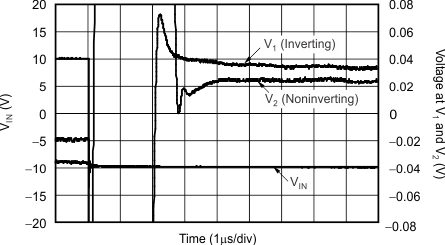
| See the Settling Time section. The grid for voltage at V1 and V2 is scaled 20 mV or 0.1% per division. | ||
| 20-V Step | Gain = 1 | RF = 10 kΩ |
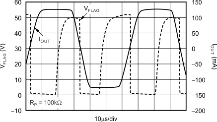
| The OPA454 was connected to sufficient heatsinking to prevent thermal shutdown. | ||
| TP = 25°C | ||
