SBOS376I November   2006  – July 2016 OPA827

PRODUCTION DATA.  

  1. Features
  2. Applications
  3. Description
  4. Revision History
  5. Pin Configuration and Functions
  6. Specifications
    1. 6.1 Absolute Maximum Ratings
    2. 6.2 ESD Ratings
    3. 6.3 Recommended Operating Conditions
    4. 6.4 Thermal Information
    5. 6.5 Electrical Characteristics
    6. 6.6 Typical Characteristics
  7. Detailed Description
    1. 7.1 Overview
    2. 7.2 Functional Block Diagram
    3. 7.3 Feature Description
      1. 7.3.1 Operating Voltage
      2. 7.3.2 Noise Performance
      3. 7.3.3 Basic Noise Calculations
      4. 7.3.4 Total Harmonic Distortion Measurements
      5. 7.3.5 Capacitive Load and Stability
      6. 7.3.6 Phase-Reversal Protection
      7. 7.3.7 Transimpedance Amplifier
        1. 7.3.7.1 Key Transimpedance Points
    4. 7.4 Device Functional Modes
  8. Application and Implementation
    1. 8.1 Application Information
    2. 8.2 Typical Application
      1. 8.2.1 Design Requirements
      2. 8.2.2 Detailed Design Procedure
      3. 8.2.3 Application Curve
    3. 8.3 System Examples
      1. 8.3.1 OPA827 Used as an I/V Converter
  9. Power Supply Recommendations
  10. 10Layout
    1. 10.1 Layout Guidelines
    2. 10.2 Layout Example
  11. 11Device and Documentation Support
    1. 11.1 Device Support
      1. 11.1.1 Third-Party Products Disclaimer
      2. 11.1.2 Development Support
    2. 11.2 Documentation Support
      1. 11.2.1 Related Documentation
    3. 11.3 Receiving Notification of Documentation Updates
    4. 11.4 Community Resource
    5. 11.5 Trademarks
    6. 11.6 Electrostatic Discharge Caution
    7. 11.7 Glossary
  12. 12Mechanical, Packaging, and Orderable Information
Package Options

Mechanical Data (Package|Pins)
Thermal pad, mechanical data (Package|Pins)
Orderable Information

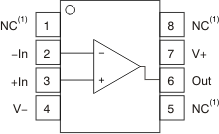
5 Pin Configuration and Functions

D and DGK Packages
8-Pin SOIC and VSSOP
Top View
OPA827 po_so_msop_bos376.gif
1. NC denotes no internal connection.

Pin Functions

PIN I/O DESCRIPTION
NO. NAME
+IN 3 I Noninverting input
–IN 2 I Inverting input
NC 1, 5, 8 No internal connection (can be left floating)
OUT 6 O Output
V+ 7 Positive power supply
V– 4 Negative power supply