SBOS813 August 2016 OPA857-DIE
PRODUCTION DATA.
Package Options
Mechanical Data (Package|Pins)
- TD|0
Thermal pad, mechanical data (Package|Pins)
Orderable Information
5 Bare Die Information
| DIE THICKNESS | BACKSIDE FINISH | BACKSIDE POTENTIAL |
BOND PAD METALLIZATION COMPOSITION |
BOND PAD THICKNESS |
|---|---|---|---|---|
| 15 mils. | Silicon with backgrind | GND | TiW/AlCu (0.5%) | 1100 nm |

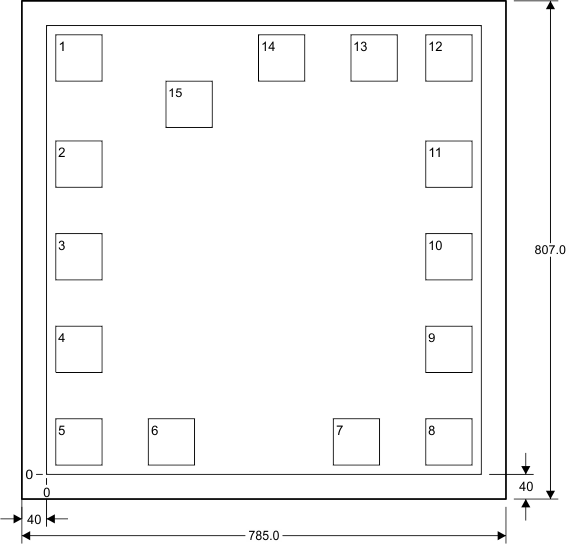
Bond Pad Coordinates in Microns
| NAME | PAD NUMBER | X MIN | Y MIN | X MAX | Y MAX | DESCRIPTION |
|---|---|---|---|---|---|---|
| GND | 1 | 15 | 637 | 90 | 712 | Ground |
| CTRL | 2 | 15 | 465 | 90 | 540 | Control pin for transimpedance gain. GND, logic 0 = 5-kΩ internal resistance; +VS, logic 1 = 20-kΩ internal resistance. |
| GND | 3 | 15 | 315 | 90 | 390 | Ground |
| GND | 4 | 15 | 165 | 90 | 240 | Ground |
| OUTN | 5 | 15 | 15 | 90 | 90 | Common-mode voltage output reference |
| GND | 6 | 165 | 15 | 240 | 90 | Ground |
| GND | 7 | 465 | 15 | 540 | 90 | Ground |
| OUT | 8 | 615 | 15 | 690 | 90 | Signal output |
| +VS | 9 | 615 | 165 | 690 | 240 | Supply voltage |
| +VS | 10 | 615 | 315 | 690 | 390 | Supply voltage |
| +VS | 11 | 615 | 465 | 690 | 540 | Supply voltage |
| GND | 12 | 615 | 637 | 690 | 712 | Ground |
| TESD_SD | 13 | 493.7 | 637 | 568.7 | 712 | Test mode enable. Connect to GND for normal operation, and connect to +VS to enable test mode. |
| TEST_IN | 14 | 343.7 | 637 | 418.7 | 712 | Test mode input. Connect to +VS during normal operation. |
| IN | 15 | 193.7 | 561.95 | 268.7 | 636.95 | Input |