SCPS148I October 2005 – June 2022 PCA9546A
PRODUCTION DATA
- 1 Features
- 2 Applications
- 3 Description
- 4 Revision History
- 5 Pin Configuration and Functions
- 6 Specifications
- 7 Parameter Measurement Information
- 8 Detailed Description
- 9 Application Information Disclaimer
- 10Power Supply Recommendations
- 11Layout
- 12Device and Documentation Support
- 13Mechanical, Packaging, and Orderable Information
5 Pin Configuration and Functions
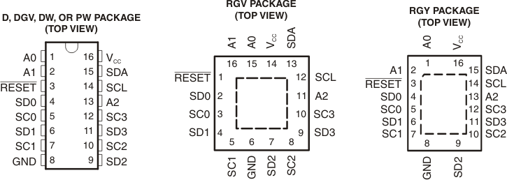
Table 5-1 Pin Functions
| PIN | DESCRIPTION | ||
|---|---|---|---|
| NAME | NO. | ||
| D, DGV, DW, PW, AND RGY | RGV | ||
| A0 | 1 | 15 | Address input 0. Connect directly to VCC or ground |
| A1 | 2 | 16 | Address input 1. Connect directly to VCC or ground |
| A2 | 13 | 11 | Address input 2. Connect directly to VCC or ground |
| GND | 8 | 6 | Ground |
| RESET | 3 | 1 | Active low reset input. Connect to VDPUM(1) through a pull-up resistor, if not used. |
| SD0 | 4 | 2 | Serial data 0. Connect to VDPU0(1) through a pull-up resistor |
| SC0 | 5 | 3 | Serial clock 0. Connect to VDPU0(1) through a pull-up resistor |
| SD1 | 6 | 4 | Serial data 1. Connect to VDPU1(1) through a pull-up resistor |
| SC1 | 7 | 5 | Serial clock 1. Connect to VDPU1(1) through a pull-up resistor |
| SD2 | 9 | 7 | Serial data 2. Connect to VDPU2(1) through a pull-up resistor |
| SC2 | 10 | 8 | Serial clock 2. Connect to VDPU2(1) through a pull-up resistor |
| SD3 | 11 | 9 | Serial data 3. Connect to VDPU3(1) through a pull-up resistor. |
| SC3 | 12 | 10 | Serial clock 3. Connect to VDPU3(1) through a pull-up resistor |
| SCL | 14 | 12 | Serial clock line. Connect to VDPUM(1) through a pull-up resistor |
| SDA | 15 | 13 | Serial data line. Connect to VDPUM(1) through a pull-up resistor |
| VCC | 16 | 14 | Supply power |
(1) VDPUX is the pull-up reference voltage for the
associated data line. VDPUM is the master I2C reference
voltage while VDPU0 - VDPU3 are the slave channel
reference voltages.