SBAS451B October 2008 – August 2015 PCM1789
PRODUCTION DATA.
- 1 Features
- 2 Applications
- 3 Description
- 4 Revision History
- 5 Pin Configuration and Functions
-
6 Specifications
- 6.1 Absolute Maximum Ratings
- 6.2 ESD Ratings
- 6.3 Recommended Operating Conditions
- 6.4 Thermal Information
- 6.5 Electrical Characteristics: Digital Input/Output
- 6.6 Electrical Characteristics: DAC
- 6.7 Electrical Characteristics: Power-Supply Requirements
- 6.8 System Clock Timing Requirements
- 6.9 Audio Interface Timing Requirements
- 6.10 Three-Wire Timing Requirements
- 6.11 SCL and SDA Timing Requirements
- 6.12 Typical Characteristics
-
7 Detailed Description
- 7.1 Overview
- 7.2 Functional Block Diagram
- 7.3
Feature Description
- 7.3.1 Analog Outputs
- 7.3.2 Voltage Reference VCOM
- 7.3.3 System Clock Input
- 7.3.4 Reset Operation
- 7.3.5 ZERO Flag
- 7.3.6 AMUTE Control
- 7.3.7 Three-Wire (SPI) Serial Control
- 7.3.8 Control Data Word Format
- 7.3.9 Register Write Operation
- 7.3.10 Timing Requirements
- 7.3.11 Two-wire (I2C) Serial Control
- 7.3.12 Packet Protocol
- 7.3.13 Write Operation
- 7.3.14 Read Operation
- 7.4 Device Functional Modes
- 7.5 Register Maps
- 8 Application and Implementation
- 9 Power Supply Recommendations
- 10Layout
- 11Device and Documentation Support
- 12Mechanical, Packaging, and Orderable Information
Package Options
Mechanical Data (Package|Pins)
- PW|24
Thermal pad, mechanical data (Package|Pins)
Orderable Information
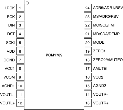
5 Pin Configuration and Functions
PW Package
24-Pin TSSOP
Top View

Pin Functions
| PIN | I/O | PULL-DOWN | 5-V TOLERANT | DESCRIPTION | |
|---|---|---|---|---|---|
| NAME | NO. | ||||
| LRCK | 1 | I | Yes | No | Audio data word clock input |
| BCK | 2 | I | Yes | No | Audio data bit clock input |
| DIN | 3 | I | No | No | Audio data input |
| RST | 4 | I | Yes | Yes | Reset and power-down control input with active low |
| SCKI | 5 | I | No | Yes | System clock input |
| VDD | 6 | — | — | — | Digital power supply, +3.3 V |
| DGND | 7 | — | — | — | Digital ground |
| VCC1 | 8 | — | — | — | Analog power supply 1, +5 V |
| VCOM | 9 | — | — | — | Voltage common decoupling |
| AGND1 | 10 | — | — | — | Analog ground 1 |
| VOUTL– | 11 | O | No | No | Negative analog output from DAC left channel |
| VOUTL+ | 12 | O | No | No | Positive analog output from DAC left channel |
| VOUTR+ | 13 | O | No | No | Positive analog output from DAC right channel |
| VOUTR– | 14 | O | No | No | Negative analog output from DAC right channel |
| AGND2 | 15 | — | — | — | Analog ground 2 |
| VCC2 | 16 | — | — | — | Analog power supply 2, +5 V |
| AMUTEI | 17 | I | No | Yes | Analog mute control input with active low |
| ZERO2/AMUTEO | 18 | O | No | No | Zero detect flag output 2/Analog mute control output(1) with active low |
| ZERO1 | 19 | O | No | No | Zero detect flag output 1 |
| MODE | 20 | I | No | No | Control port mode selection. Tied to VDD: SPI, ADR6 = 1, pull-up: SPI, ADR6 = 0, pull-down: H/W auto mode, tied to DGND: I2C |
| MD/SDA/DEMP | 21 | I/O | No | Yes | Input data for SPI, data for I2C(1), de-emphasis control for hardware control mode |
| MC/SCL/FMT | 22 | I | No | Yes | Clock for SPI, clock for I2C, format select for hardware control mode |
| MS/ADR0/RSV | 23 | I | Yes | Yes | Chip Select for SPI, address select 0 for I2C, reserve (set low) for hardware control mode |
| ADR5/ADR1/RSV | 24 | I | No | Yes | Address select 5 for SPI, address select 1 for I2C, reserve (set low) for hardware control mode |
(1) Open-drain configuration in out mode.