SBFS038A June 2012 – September 2015 PCM2903C
PRODUCTION DATA.
- 1 Features
- 2 Applications
- 3 Description
- 4 Revision History
- 5 Device Comparison Table
- 6 Pin Configuration and Functions
-
7 Specifications
- 7.1 Absolute Maximum Ratings
- 7.2 ESD Ratings
- 7.3 Recommended Operating Conditions
- 7.4 Thermal Information
- 7.5 Electrical Characteristics
- 7.6
Typical Characteristics
- 7.6.1 Typical Characteristics: ADC
- 7.6.2 Typical Characteristics: DAC
- 7.6.3 Typical Characteristics: ADC Output Spectrum
- 7.6.4 Typical Characteristics: DAC Output Spectrum
- 7.6.5 Typical Characteristics: Supply Current
- 7.6.6 Typical Characteristics: ADC Digital Decimation Filter Frequency Response
- 7.6.7 Typical Characteristics: ADC Digital High-Pass Filter Frequency Response
- 7.6.8 Typical Characteristics: ADC Analog Antialiasing Filter Frequency Response
- 7.6.9 Typical Characteristics: DAC Digital Interpolation Filter Frequency Response
- 7.6.10 Typical Characteristics: DAC Analog Fir Filter Frequency Response
- 7.6.11 Typical Characteristics: DAC Analog Low-Pass Filter Frequency Response
- 8 Parameter Measurement Information
- 9 Detailed Description
- 10Application and Implementation
- 11Power Supply Recommendations
- 12Layout
- 13Device and Documentation Support
- 14Mechanical, Packaging, and Orderable Information
Package Options
Mechanical Data (Package|Pins)
- DB|28
Thermal pad, mechanical data (Package|Pins)
Orderable Information
7 Specifications
7.1 Absolute Maximum Ratings
Over operating free-air temperature range (unless otherwise noted).(1)| MIN | MAX | UNIT | ||
|---|---|---|---|---|
| Supply voltage, VCCC, VCCP1, VCCP2, VCCX, VDD | –0.3 | 4 | V | |
| Supply voltage differences, VCCC, VCCP1, VCCP2, VCCX, VDD | ±0.1 | V | ||
| Ground voltage differences, AGNDC, AGNDP, AGNDX, DGND, DGNDU | ±0.1 | V | ||
| Digital input voltage | SEL0, SEL1, DIN | –0.3 | 6.5 | V |
| D+, D–, HID0, HID1, HID2, XTI, XTO, DOUT, SSPND | –0.3 | (VDD + 0.3) < 4 | V | |
| Analog input voltage VINL, VINR, VCOM, VOUTR, VOUTL | –0.3 | (VCCC + 0.3) < 4 | V | |
| Input current (any pins except supplies) | ±10 | mA | ||
| Ambient temperature under bias | –40 | 125 | °C | |
| Junction temperature TJ | 150 | °C | ||
| Lead temperature (soldering, 5 s) | 260 | °C | ||
| Package temperature (IR reflow, peak) | 250 | °C | ||
| Storage temperature, Tstg | –55 | 150 | °C | |
(1) Stresses beyond those listed under Absolute Maximum Ratings may cause permanent damage to the device. These are stress ratings only, which do not imply functional operation of the device at these or any other conditions beyond those indicated under Recommended Operating Conditions. Exposure to absolute-maximum-rated conditions for extended periods may affect device reliability.
7.2 ESD Ratings
| VALUE | UNIT | |||
|---|---|---|---|---|
| V(ESD) | Electrostatic discharge | Human-body model (HBM), per ANSI/ESDA/JEDEC JS-001(1) | ±2500 | V |
| Charged-device model (CDM), per JEDEC specification JESD22-C101(2) | ±1000 | |||
(1) JEDEC document JEP155 states that 500-V HBM allows safe manufacturing with a standard ESD control process.
(2) JEDEC document JEP157 states that 250-V CDM allows safe manufacturing with a standard ESD control process.
7.3 Recommended Operating Conditions
over operating free-air temperature range (unless otherwise noted)| MIN | NOM | MAX | UNIT | ||
|---|---|---|---|---|---|
| Supply voltage | 3 | 3.3 | 3.6 | V | |
| Supply current | ADC, DAC operation | 54 | 70 | mA | |
| USB suspend state | 250 | µA | |||
| Ambient temperature | 0 | 25 | 85 | °C | |
7.4 Thermal Information
| THERMAL METRIC(1) | PCM2903C | UNIT | |
|---|---|---|---|
| DB (SSOP) | |||
| 28 PINS | |||
| RθJA | Junction-to-ambient thermal resistance | 64.5 | °C/W |
| RθJC(top) | Junction-to-case (top) thermal resistance | 24.5 | °C/W |
| RθJB | Junction-to-board thermal resistance | 25.4 | °C/W |
| ψJT | Junction-to-top characterization parameter | 2.0 | °C/W |
| ψJB | Junction-to-board characterization parameter | 25 | °C/W |
| RθJC(bot) | Junction-to-case (bottom) thermal resistance | — | °C/W |
(1) For more information about traditional and new thermal metrics, see the Semiconductor and IC Package Thermal Metrics application report, SPRA953.
7.5 Electrical Characteristics
All specifications at TA = 25°C, VCCC = VCCP1 = VCCP2 = VCCX = VDD = 3.3 V, fS = 44.1 kHz, fIN = 1 kHz, 16-bit data, unless otherwise noted.| PARAMETER | TEST CONDITIONS | MIN | TYP | MAX | UNIT | ||
|---|---|---|---|---|---|---|---|
| DIGITAL INPUT/OUTPUT | |||||||
| Host interface | Apply USB Revision 2.0, full speed | ||||||
| Audio data format | USB isochronous data format | ||||||
| INPUT LOGIC | |||||||
| VIH | High-level input voltage | D+, D– | 2 | VDD | VDC | ||
| XTI, HID0, HID1, and HID2 | 0.7 VDD | VDD | |||||
| SEL0, SEL1 | 2 | 5.25 | |||||
| DIN | 0.7 VDD | 5.25 | |||||
| VIL | Low-level input voltage | D+, D– | 0.8 | VDC | |||
| XTI, HID0, HID1, and HID2 | 0.3 VDD | ||||||
| SEL0, SEL1 | 0.8 | ||||||
| DIN | 0.3 VDD | ||||||
| IIH | High-level input current | D+, D–, XTI, SEL0, SEL1 | VIN = 3.3 V | ±10 | μA | ||
| HID0, HID1, and HID2 | VIN = 3.3 V | 50 | 80 | ||||
| DIN | VIN = 3.3 V | 65 | 100 | ||||
| IIL | Low-level input current | D+, D–, XTI, SEL0, SEL1 | VIN = 0 V | ±10 | μA | ||
| HID0, HID1, and HID2 | VIN = 0 V | ±10 | |||||
| DIN | VIN = 0 V | ±10 | |||||
| OUTPUT LOGIC | |||||||
| VOH | High-level output voltage | D+, D– | 2.8 | VDC | |||
| DOUT | IOH = –4 mA | 2.8 | |||||
| SSPND | IOH = –2 mA | 2.8 | |||||
| VOL | Low-level output voltage | D+, D– | 0.3 | VDC | |||
| DOUT | IOL = 4 mA | 0.5 | |||||
| SSPND | IOL = 2 mA | 0.5 | |||||
| CLOCK FREQUENCY | |||||||
| Input clock frequency, XTI | 11.994 | 12 | 12.006 | MHz | |||
| ADC CHARACTERISTICS | |||||||
| Resolution | 8, 16 | Bits | |||||
| Audio data channel | 1, 2 | Channel | |||||
| ADC CLOCK FREQUENCY | |||||||
| fS | Sampling frequencies | 8, 11.025, 16, 22.05, 32, 44.1, 48 | kHz | ||||
| ADC DC ACCURACY | |||||||
| Gain mismatch, channel-to-channel | ±1 | ±5 | % of FSR | ||||
| Gain error | ±2 | ±10 | % of FSR | ||||
| Bipolar zero error | ±0 | % of FSR | |||||
| ADC DYNAMIC PERFORMANCE(1) | |||||||
| THD+N | Total harmonic distortion plus noise | VIN = –1 dB | 0.01% | 0.02% | |||
| VIN = –60 dB | 5% | ||||||
| Dynamic range | A-weighted | 81 | 89 | dB | |||
| SNR | Signal-to-noise ratio | A-weighted | 81 | 89 | dB | ||
| Channel separation | 80 | 85 | dB | ||||
| ANALOG INPUT | |||||||
| Input voltage | 0.6 VCCC | VPP | |||||
| Center voltage | 0.5 VCCC | V | |||||
| Input impedance | 30 | kΩ | |||||
| Antialising filter frequency response | –3 dB | 150 | kHz | ||||
| fIN = 20 kHz | –0.08 | dB | |||||
| ADC DIGITAL FILTER PERFORMANCE | |||||||
| Passband | 0.454 fS | Hz | |||||
| Stop band | 0.583 fS | Hz | |||||
| Passband ripple | ±0.05 | dB | |||||
| Stop-band attenuation | –65 | dB | |||||
| td | Delay time | 17.4/fS | s | ||||
| HPF frequency response | –3 dB | 0.078 fS/1000 | Hz | ||||
| DAC CHARACTERISTICS | |||||||
| Resolution | 8, 16 | Bits | |||||
| Audio data channel | 1, 2 | Channel | |||||
| DAC CLOCK FREQUENCY | |||||||
| fS | Sampling frequencies | 32, 44.1, 48 | kHz | ||||
| DAC DC ACCURACY | |||||||
| Gain mismatch channel-to-channel | ±1 | ±5 | % of FSR | ||||
| Gain error | ±2 | ±10 | % of FSR | ||||
| Bipolar zero error | ±2 | % of FSR | |||||
| DAC DYNAMIC PERFORMANCE(2) | |||||||
| THD+N | Total harmonic distortion plus noise | VOUT = 0 dB | 0.005% | 0.016% | |||
| VOUT = –60 dB | 3% | ||||||
| Dynamic range | EIAJ, A-weighted | 87 | 93 | dB | |||
| SNR | Signal-to-noise ratio | EIAJ, A-weighted | 90 | 96 | dB | ||
| Channel separation | 86 | 92 | dB | ||||
| ANALOG OUTPUT | |||||||
| VO | Output voltage | 0.6 VCCC | VPP | ||||
| Center voltage | 0.5 VCCC | V | |||||
| Load impedance | AC coupling | 10 | kΩ | ||||
| LPF frequency response | –3 dB | 250 | kHz | ||||
| f = 20 kHz | –0.03 | dB | |||||
| DAC DIGITAL FILTER PERFORMANCE | |||||||
| Passband | 0.445 fS | Hz | |||||
| Stop band | 0.555 fS | Hz | |||||
| Passband ripple | ±0.1 | dB | |||||
| Stop-band attenuation | –43 | dB | |||||
| td | Delay time | 14.3/fS | s | ||||
| POWER-SUPPLY REQUIREMENTS | |||||||
| VDD, VCCC, VCCP1, VCCP2, VCCX | Voltage range | 3 | 3.3 | 3.6 | VDC | ||
| Supply current | ADC, DAC operation | 54 | 70 | mA | |||
| Suspend mode(3) | 250 | μA | |||||
| PD | Power dissipation | ADC, DAC operation | 178 | 252 | mW | ||
| Suspend mode(3) | 0.83 | mW | |||||
| TEMPERATURE RANGE | |||||||
| Operating temperature range | –25 | 85 | °C | ||||
(1) fIN = 1 kHz, using a System Two™ audio measurement system by Audio Precision™ in RMS mode with a 20-kHz LPF and 400-Hz HPF in the calculation.
(2) fOUT = 1 kHz, using a System Two audio measuerment system by Audio Precision in RMS mode with a 20-kHz LPF and 400-Hz HPF.
(3) Under USB suspend state.
7.6 Typical Characteristics
7.6.1 Typical Characteristics: ADC
All specifications at TA = +25°C, VDD = VCCC = VCCP1 = VCCP2 = VCCx = 3.3 V, fs = 44.1 kHz, fIN = 1 kHz, 16-bit data, unless otherwise noted.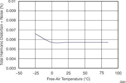 Figure 1. Total Harmonic Distortion + Noise at –1 dB vs Free-Air Temperature
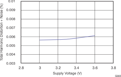 Figure 3. Total Harmonic Distortion + Noise at –1 dB vs Supply Voltage
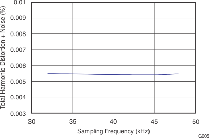 Figure 5. Total Harmonic Distortion + Noise at –1 dB vs Sampling Frequency
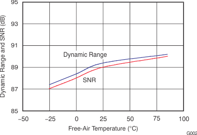 Figure 2. Dynamic Range and SNR vs Free-Air Temperature
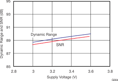 Figure 4. Dynamic Range and SNR vs Supply Voltage
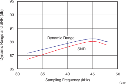 Figure 6. Dynamic Range and SNR vs Sampling Frequency
7.6.2 Typical Characteristics: DAC
All specifications at TA = +25°C, VDD = VCCC = VCCP1 = VCCP2 = VCCx = 3.3 V, fs = 44.1 kHz, fIN = 1 kHz, 16-bit data, unless otherwise noted.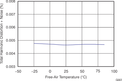 Figure 7. Total Harmonic Distortion + Noise at 0 dB vs Free-Air Temperature
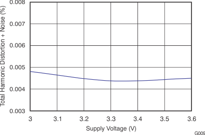 Figure 9. Total Harmonic Distortion + Noise at 0 dB vs Supply Voltage
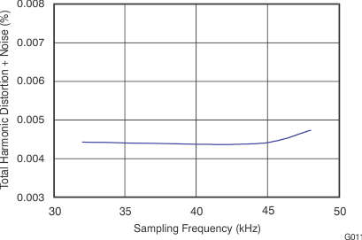 Figure 11. Total Harmonic Distortion + Noise at 0 dB vs Sampling Frequency
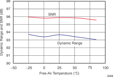 Figure 8. Dynamic Range and SNR vs Free-Air Temperature
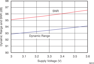 Figure 10. Dynamic Range and SNR vs Supply Voltage
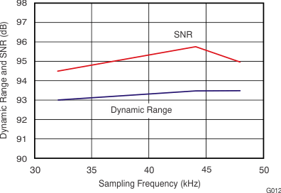 Figure 12. Dynamic Range and SNR vs Sampling Frequency
7.6.3 Typical Characteristics: ADC Output Spectrum
All specifications at TA = 25°C, VDD = VCCC = VCCP1 = VCCP2 = VCCx = 3.3 V, fs = 44.1 kHz, fIN = 1 kHz, 16-bit data, unless otherwise noted.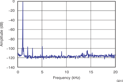 Figure 13. Output Spectrum (–1 dB, N = 8192)
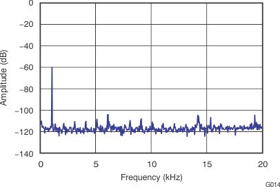 Figure 14. Output Spectrum (–60 dB, N = 8192)
7.6.4 Typical Characteristics: DAC Output Spectrum
All specifications at TA = 25°C, VDD = VCCC = VCCP1 = VCCP2 = VCCx = 3.3 V, fs = 44.1 kHz, fIN = 1 kHz, 16-bit data, unless otherwise noted.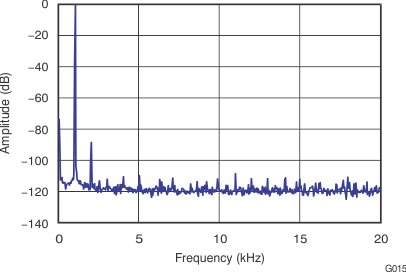 Figure 15. Output Spectrum (0 dB, N = 8192)
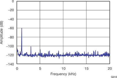 Figure 16. Output Spectrum (–60 dB, N = 8192)
7.6.5 Typical Characteristics: Supply Current
All specifications at TA = 25°C, VDD = VCCC = VCCP1 = VCCP2 = VCCx = 3.3 V, fs = 44.1 kHz, fIN = 1 kHz, 16-bit data, unless otherwise noted.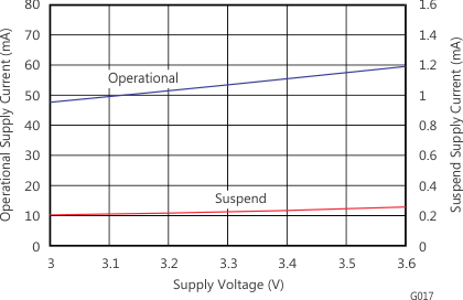 Figure 17. Operational and Suspend Supply Current vs Supply Voltage
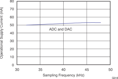 Figure 18. Operational Supply Current vs Sampling Frequency
7.6.6 Typical Characteristics: ADC Digital Decimation Filter Frequency Response
All specifications at TA = 25°C, VDD = VCCC = VCCP1 = VCCP2 = VCCx = 3.3 V, fs = 44.1 kHz, fIN = 1 kHz, 16-bit data, unless otherwise noted.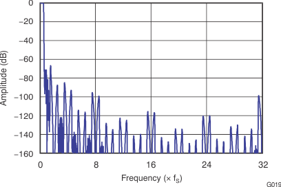 Figure 19. Overall Characteristics
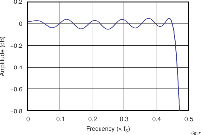 Figure 21. Passband Ripple
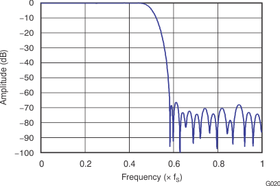 Figure 20. Stop-Band Attenuation
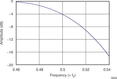 Figure 22. Transition-Band Response
7.6.7 Typical Characteristics: ADC Digital High-Pass Filter Frequency Response
All specifications at TA = 25°C, VDD = VCCC = VCCP1 = VCCP2 = VCCx = 3.3 V, fs = 44.1 kHz, fIN = 1 kHz, 16-bit data, unless otherwise noted.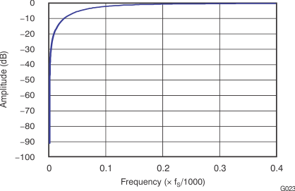 Figure 23. Stop-Band Characteristics
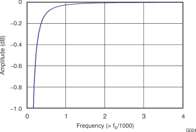 Figure 24. Passband Characteristics
7.6.8 Typical Characteristics: ADC Analog Antialiasing Filter Frequency Response
All specifications at TA = 25°C, VDD = VCCC = VCCP1 = VCCP2 = VCCx = 3.3 V, fs = 44.1 kHz, fIN = 1 kHz, 16-bit data, unless otherwise noted.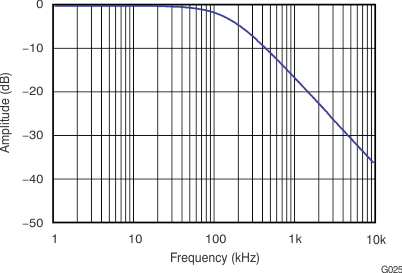 Figure 25. Stop-Band Characteristics
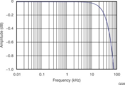 Figure 26. Passband Characteristics
7.6.9 Typical Characteristics: DAC Digital Interpolation Filter Frequency Response
All specifications at TA = 25°C, VDD = VCCC = VCCP1 = VCCP2 = VCCx = 3.3 V, fs = 44.1 kHz, fIN = 1 kHz, 16-bit data, unless otherwise noted.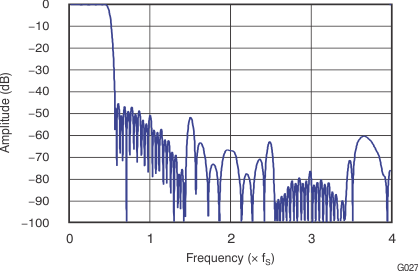 Figure 27. Stop-Band Attenuation
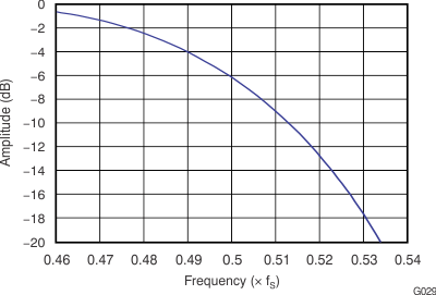 Figure 29. Transition-Band Response
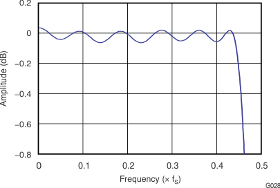 Figure 28. Passband Ripple
7.6.10 Typical Characteristics: DAC Analog Fir Filter Frequency Response
All specifications at TA = 25°C, VDD = VCCC = VCCP1 = VCCP2 = VCCx = 3.3 V, fs = 44.1 kHz, fIN = 1 kHz, 16-bit data, unless otherwise noted.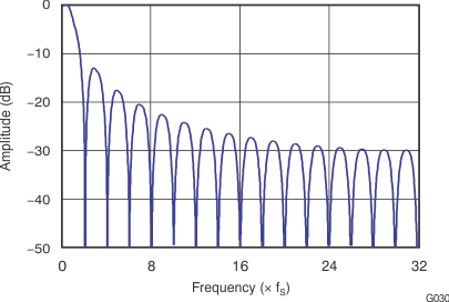 Figure 30. Stop-Band Characteristics
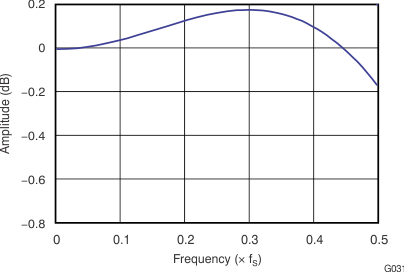 Figure 31. Passband Characteristics
7.6.11 Typical Characteristics: DAC Analog Low-Pass Filter Frequency Response
All specifications at TA = 25°C, VDD = VCCC = VCCP1 = VCCP2 = VCCx = 3.3 V, fs = 44.1 kHz, fIN = 1 kHz, 16-bit data, unless otherwise noted.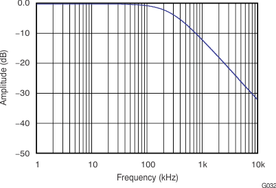 Figure 32. Stop-Band Characteristics
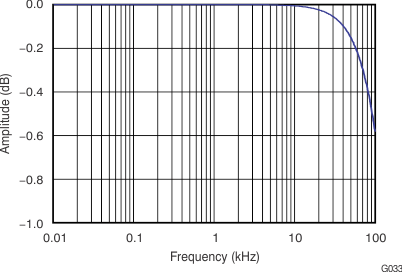 Figure 33. Passband Characteristics