SLASE12A July 2014 – October 2014 PCM5242
PRODUCTION DATA.
- 1 Features
- 2 Applications
- 3 Description
- 4 Simplified System Diagram
- 5 Revision History
- 6 Pin Configuration and Functions
- 7 Specifications
-
8 Detailed Description
- 8.1 Overview
- 8.2 Functional Block Diagram
- 8.3 Terminology
- 8.4 Audio Data Interface
- 8.5 XSMT Pin (Soft Mute / Soft Un-Mute)
- 8.6 Audio Processing
- 8.7 DAC and Differential Analog Outputs
- 8.8
Reset and System Clock Functions
- 8.8.1 Clocking Overview
- 8.8.2 Clock Slave Mode With Master Clock (SCK) Input (4 Wire I2S)
- 8.8.3 Clock Slave Mode with BCK PLL to Generate Internal Clocks (3-Wire PCM)
- 8.8.4 Clock Generation Using The PLL
- 8.8.5 PLL Calculation
- 8.8.6 Clock Master Mode from Audio Rate Master Clock
- 8.8.7 Clock Master from a Non-Audio Rate Master Clock
- 8.9 Device Functional Modes
- 9 Applications and Implementation
- 10Power Supply Recommendations
- 11Layout
-
12Programming and Registers Reference
- 12.1 Coefficient Data Formats
- 12.2
PCM5242 Register Map
- 12.2.1
Detailed Register Descriptions
- 12.2.1.1 Register Map Summary
- 12.2.1.2
Page 0 Registers
- 12.2.1.2.1 Page 0 / Register 1
- 12.2.1.2.2 Page 0 / Register 2
- 12.2.1.2.3 Page 0 / Register 3
- 12.2.1.2.4 Page 0 / Register 4
- 12.2.1.2.5 Page 0 / Register 6
- 12.2.1.2.6 Page 0 / Register 7
- 12.2.1.2.7 Page 0 / Register 8
- 12.2.1.2.8 Page 0 / Register 9
- 12.2.1.2.9 Page 0 / Register 10
- 12.2.1.2.10 Page 0 / Register 12
- 12.2.1.2.11 Page 0 / Register 13
- 12.2.1.2.12 Page 0 / Register 14
- 12.2.1.2.13 Page 0 / Register 18
- 12.2.1.2.14 Page 0 / Register 19
- 12.2.1.2.15 Page 0 / Register 20
- 12.2.1.2.16 Page 0 / Register 21
- 12.2.1.2.17 Page 0 / Register 22
- 12.2.1.2.18 Page 0 / Register 23
- 12.2.1.2.19 Page 0 / Register 24
- 12.2.1.2.20 Page 0 / Register 27
- 12.2.1.2.21 Page 0 / Register 28
- 12.2.1.2.22 Page 0 / Register 29
- 12.2.1.2.23 Page 0 / Register 30
- 12.2.1.2.24 Page 0 / Register 32
- 12.2.1.2.25 Page 0 / Register 33
- 12.2.1.2.26 Page 0 / Register 34
- 12.2.1.2.27 Page 0 / Register 35
- 12.2.1.2.28 Page 0 / Register 36
- 12.2.1.2.29 Page 0 / Register 37
- 12.2.1.2.30 Page 0 / Register 40
- 12.2.1.2.31 Page 0 / Register 41
- 12.2.1.2.32 Page 0 / Register 42
- 12.2.1.2.33 Page 0 / Register 43
- 12.2.1.2.34 Page 0 / Register 44
- 12.2.1.2.35 Page 0 / Register 59
- 12.2.1.2.36 Page 0 / Register 60
- 12.2.1.2.37 Page 0 / Register 61
- 12.2.1.2.38 Page 0 / Register 62
- 12.2.1.2.39 Page 0 / Register 63
- 12.2.1.2.40 Page 0 / Register 64
- 12.2.1.2.41 Page 0 / Register 65
- 12.2.1.2.42 Page 0 / Register 80
- 12.2.1.2.43 Page 0 / Register 81
- 12.2.1.2.44 Page 0 / Register 82
- 12.2.1.2.45 Page 0 / Register 83
- 12.2.1.2.46 Page 0 / Register 84
- 12.2.1.2.47 Page 0 / Register 85
- 12.2.1.2.48 Page 0 / Register 86
- 12.2.1.2.49 Page 0 / Register 87
- 12.2.1.2.50 Page 0 / Register 90
- 12.2.1.2.51 Page 0 / Register 91
- 12.2.1.2.52 Page 0 / Register 92
- 12.2.1.2.53 Page 0 / Register 93
- 12.2.1.2.54 Page 0 / Register 94
- 12.2.1.2.55 Page 0 / Register 95
- 12.2.1.2.56 Page 0 / Register 108
- 12.2.1.2.57 Page 0 / Register 109
- 12.2.1.2.58 Page 0 / Register 114
- 12.2.1.2.59 Page 0 / Register 115
- 12.2.1.2.60 Page 0 / Register 118
- 12.2.1.2.61 Page 0 / Register 119
- 12.2.1.2.62 Page 0 / Register 120
- 12.2.1.2.63 Page 0 / Register 121
- 12.2.1.2.64 Page 0 / Register 122
- 12.2.1.2.65 Page 0 / Register 123
- 12.2.1.2.66 Page 0 / Register 124
- 12.2.1.2.67 Page 0 / Register 125
- 12.2.1.3 Page 1 Registers
- 12.2.1.4 Page 44 Registers
- 12.2.1.5 Page 253 Registers
- 12.2.2 PLL Tables for Software Controlled Devices
- 12.2.1
Detailed Register Descriptions
- 13Device and Documentation Support
- 14Mechanical, Packaging, and Orderable Information
Package Options
Mechanical Data (Package|Pins)
- RHB|32
Thermal pad, mechanical data (Package|Pins)
- RHB|32
Orderable Information
7 Specifications
7.1 Absolute Maximum Ratings
over operating free-air temperature range (unless otherwise noted)| MIN | MAX | UNIT | ||
|---|---|---|---|---|
| Supply Voltage | AVDD, CPVDD, DVDD | –0.3 | 3.9 | V |
| LDOO wtih DVDD at 1.8V | –0.3 | 2.25 | ||
| Digital Input Voltage | DVDD at 1.8V | –0.3 | 2.25 | |
| DVDD at 3.3V | –0.3 | 3.9 | ||
| Analog Input Voltage | –0.3 | 3.9 | ||
7.2 Handling Ratings
| MIN | MAX | UNIT | |||
|---|---|---|---|---|---|
| Tstg | Storage Temperature | –40 | 125 | °C | |
| V(ESD) | Electrostatic Discharge | Human body model (HBM), per ANSI/ESDA/JEDEC JS-001, all pins(1) | –2500 | 2500 | V |
| Charged device model (CDM), per JEDEC specification JESD22-C101, all pins | –1500 | 1500 | |||
(1) Level listed above is the passing level per ANSI, ESDA, and JEDEC JS-001. JEDEC document JEP155 states that 500V HBM allows safe manufacturing with a standard ESD control process.
7.3 Recommended Operating Conditions
| MIN | NOM | MAX | UNIT | ||||
|---|---|---|---|---|---|---|---|
| AVDD | Analog power supply voltage range | Referenced to AGND(1) | VCOM mode | 3.0 | 3.3 | 3.46 | V |
| VREF mode | 3.2 | 3.3 | 3.46 | ||||
| DVDD | Digital power supply voltage range | Referenced to DGND(1) | 1.8V DVDD | 1.65 | 1.8 | 1.95 | V |
| 3.3V DVDD | 3.1 | 3.3 | 3.46 | ||||
| CPVDD | Charge pump supply voltage range | Referenced to CPGND(1) | 3.1 | 3.3 | 3.46 | V | |
| MCLK | Master Clock Frequency | 50 | MHz | ||||
| LOL, LOR | Stereo line output load resistance | 2 | 10 | kΩ | |||
| CLout | Digital output load capacitance | 10 | pF | ||||
| TJ | Operating Junction Temperature Range | –25 | 85 | °C | |||
(1) All grounds on board are tied together; they must not differ in voltage by more than 0.2V max, for any combination of ground signals.
7.4 Thermal Information
| THERMAL METRIC | RHB (32 PINS) | UNIT | ||
|---|---|---|---|---|
| RθJA | Junction-to-ambient thermal resistance | 72.2 | °C/W | |
| RθJC(top) | Junction-to-case(top) thermal resistance | 17.5 | ||
| RθJB | Junction-to-board thermal resistance | 35.0 | ||
| ψJT | Junction-to-top characterization parameter | 0.4 | ||
| ψJB | Junction-to-board characterization parameter | 34.5 | ||
| RθJC(bottom) | Junction-to-case(bottom) thermal resistance | n/a | ||
7.5 Electrical Characteristics
All specifications at TA = 25°C, AVDD = CPVDD = DVDD = 3.3V, fS = 48kHz, system clock = 512fS and 24-bit data unless otherwise noted.| PARAMETER | TEST CONDITIONS | MIN | TYP | MAX | UNIT | |
|---|---|---|---|---|---|---|
| Resolution | 16 | 24 | 32 | Bits | ||
| Digital Input/Output | ||||||
| Logic Family: 3.3V LVCMOS compatible | ||||||
| VIH | Input logic level | 0.7×DVDD | V | |||
| VIL | 0.3×DVDD | |||||
| IIH | Input logic current | VIN = VDD | 10 | µA | ||
| IIL | VIN = 0V | –10 | ||||
| VOH | Output logic level | IOH = –4mA | 0.8×DVDD | V | ||
| VOL | IOL = 4mA | 0.22×DVDD | ||||
| Logic Family 1.8V LVCMOS compatible | ||||||
| VIH | Input logic level | 0.7×DVDD | V | |||
| VIL | 0.3×DVDD | |||||
| IIH | Input logic current | VIN = VDD | 10 | µA | ||
| IIL | VIN = 0V | –10 | ||||
| VOH | Output logic level | IOH = –2mA | 0.8×DVDD | V | ||
| VOL | IOL = 2mA | 0.22×DVDD | ||||
| Dynamic Performance (PCM Mode)(1)(2) | ||||||
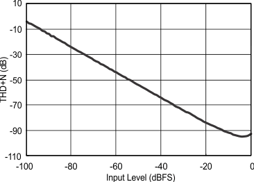
| THD+N at -1 dB(2) | fS = 48kHz | –94 | –87 | dB | ||
| fS = 96kHz | –94 | |||||
| fS = 192kHz | –94 | |||||
| Dynamic range(2) | EIAJ, A-weighted, fS = 48kHz | 108 | 114 | |||
| EIAJ, A-weighted, fS = 96kHz | 114 | |||||
| EIAJ, A-weighted, fS = 192kHz | 114 | |||||
| Signal-to-noise ratio(2) | EIAJ, A-weighted, fS = 48kHz | 114 | ||||
| EIAJ, A-weighted, fS = 96kHz | 114 | |||||
| EIAJ, A-weighted, fS = 192kHz | 114 | |||||
| Signal to noise ratio with analog mute(2)(3) | EIAJ, A-weighted, fS = 48kHz | 113 | 123 | |||
| EIAJ, A-weighted, fS = 96kHz | 113 | 123 | ||||
| EIAJ, A-weighted, fS = 192kHz | 113 | 123 | ||||
| Channel Separation | fS = 48kHz | 100 / 95 | 109 / 103 | dB | ||
| fS = 96kHz | 100 / 95 | 109 / 103 | ||||
| fS = 192kHz | 100 / 95 | 109 / 103 | ||||
| Analog Output | ||||||
| Single Ended Output voltage | 2.1 | VRMS | ||||
| Differential Output Voltage | 4.2 | VRMS | ||||
| Gain error | –6 | ±2.0 | 6 | % of FSR | ||
| Gain mismatch, channel-to-channel | –6 | ±0.5 | 6 | % of FSR | ||
| Bipolar zero error | At bipolar zero | –2 | ±1.0 | 2 | mV | |
| Load impedance | 5 | kΩ | ||||
| Filter Characteristics–1: Normal (8x) | ||||||
| Pass band | 0.45fS | kHz | ||||
| Stop band | 0.55fS | |||||
| Stop band attenuation | –60 | dB | ||||
| Pass-band ripple | ±0.02 | |||||
| Delay time | 20tS | s | ||||
| Filter Characteristics–2: Low Latency (8x) | ||||||
| Pass band | 0.47fS | kHz | ||||
| Stop band | 0.55fS | |||||
| Stop band attenuation | –52 | dB | ||||
| Pass-band ripple | ±0.0001 | |||||
| Delay time | 3.5tS | s | ||||
| Filter Characteristics–3: Asymmetric FIR (8x) | ||||||
| Pass band | 0.40fS | kHz | ||||
| Stop band | 0.72fS | |||||
| Stop band attenuation | –52 | dB | ||||
| Pass-band ripple | ±0.05 | |||||
| Delay time | 1.2tS | s | ||||
| Filter Characteristics–4: High-Attenuation (8x) | ||||||
| Pass band | 0.45fS | kHz | ||||
| Stop band | 0.45fS | |||||
| Stop band attenuation | –100 | dB | ||||
| Pass-band ripple | ±0.0005 | |||||
| Delay time | 33.7tS | s | ||||
| Power Supply Requirements | ||||||
| DVDD | Digital supply voltage | Target DVDD = 1.8V | 1.65 | 1.8 | 1.95 | VDC |
| DVDD | Digital supply voltage | Target DVDD = 3.3V | 3.0 | 3.3 | 3.6 | VDC |
| AVDD | Analog supply voltage | 3.0 | 3.3 | 3.6 | VDC | |
| CPVDD | Charge-pump supply voltage | 3.0 | 3.3 | 3.6 | VDC | |
| IDD | DVDD supply current at 1.8V | fS = 48kHz, Input is Bipolar Zero data | 11 | 14 | mA | |
| fS = 96kHz, Input is Bipolar Zero data | 12 | |||||
| fS = 192kHz, Input is Bipolar Zero data | 14 | |||||
| IDD | DVDD supply current at 1.8V | fS = 48kHz, Input is 1kHz -1dBFS data | 11 | 14 | mA | |
| fS = 96kHz, Input is 1kHz -1dBFS data | 12 | |||||
| fS = 192kHz, Input is 1kHz -1dBFS data | 14 | |||||
| IDD | DVDD supply current at 1.8V(4) | fS = N/A, Power Down Mode | 0.3 | 0.6 | mA | |
| IDD | DVDD supply current at 3.3V | fS = 48kHz, Input is Bipolar Zero data | 12 | 15 | mA | |
| fS = 96kHz, Input is Bipolar Zero data | 13 | |||||
| fS = 192kHz, Input is Bipolar Zero data | 15 | |||||
| IDD | DVDD supply current at 3.3V | fS = 48kHz, Input is 1kHz -1dBFS data | 12 | 15 | mA | |
| fS = 96kHz, Input is 1kHz -1dBFS data | 13 | |||||
| fS = 192kHz, Input is 1kHz -1dBFS data | 15 | |||||
| IDD | DVDD supply current at 3.3V(4) | fS = N/A, Power Down Mode | 0.5 | 0.8 | mA | |
| ICC | AVDD + CPVDD Supply Current | fS = 48kHz, Input is Bipolar Zero data | 11 | 16 | mA | |
| fS = 96kHz, Input is Bipolar Zero data | 11 | |||||
| fS = 192kHz, Input is Bipolar Zero data | 11 | |||||
| ICC | AVDD + CPVDD Supply Current | fS = 48kHz, Input is 1kHz -1dBFS data | 24 | 32 | mA | |
| fS = 96kHz, Input is 1kHz -1dBFS data | 24 | |||||
| fS = 192kHz, Input is 1kHz -1dBFS data | 24 | |||||
| ICC | AVDD + CPVDD Supply Current(4) | fS = N/A, Power Down Mode | 0.2 | 0.4 | mA | |
| Power Dissipation, DVDD = 1.8V | fS = 48kHz, Input is Bipolar Zero data | 59.4 | 78 | mW | ||
| fS = 96kHz, Input is Bipolar Zero data | 61.2 | |||||
| fS = 192kHz, Input is Bipolar Zero data | 64.8 | |||||
| Power Dissipation, DVDD = 1.8V | fS = 48kHz, Input is 1kHz -1dBFS data | 99 | 130.8 | mW | ||
| fS = 96kHz, Input is 1kHz -1dBFS data | 100.8 | |||||
| fS = 192kHz, Input is 1kHz -1dBFS data | 104.4 | |||||
| Power Dissipation, DVDD = 1.8V(4) | fS = N/A, Power Down Mode | 1.2 | mW | |||
| Power Dissipation, DVDD = 3.3V | fS = 48kHz, Input is Bipolar Zero data | 79.2 | 103 | mW | ||
| fS = 96kHz, Input is Bipolar Zero data | 82.5 | |||||
| fS = 192kHz, Input is Bipolar Zero data | 89.1 | |||||
| Power Dissipation, DVDD = 3.3V | fS = 48kHz, Input is 1kHz -1dBFS data | 118.8 | 155 | mW | ||
| fS = 96kHz, Input is 1kHz -1dBFS data | 122.1 | |||||
| fS = 192kHz, Input is 1kHz -1dBFS data | 128.7 | |||||
| Power Dissipation, DVDD = 3.3V(4) | fS = N/A, Power Down Mode | 2.3 | 4.0 | mW | ||
(1) Filter condition: THD+N: 20Hz HPF, 20kHz AES17 LPF Dynamic range: 20Hz HPF, 20kHz AES17 LPF, A-weighted Signal-to-noise ratio: 20Hz HPF, 20kHz AES17 LPF, A-weighted Channel separation: 20Hz HPF, 20kHz AES17 LPF Analog performance specifications are measured using the System Two Cascade™ audio measurement system by Audio Precision™ in the RMS mode.
(2) Output load is 10kΩ, with 470Ω output resistor and a 2.2nF shunt capacitor (see recommended output filter).
(3) Assert XSMT or both L-ch and R-ch PCM data are BPZ
(4) Power Down Mode, with LRCK, BCK, and SCK halted at Low level.
(5) One sample time si defined as the reciprocal of the sampling frequency. 1tS = 1/fS
(6) With the appropriate P coefficient setting, the PLL accepts up to 50MHz. This clock is then divided to meet the ≤ 20MHz requirement. See PLL Calculation.
7.6 Switching Characteristics
over operating free-air temperature range (unless otherwise noted)| PARAMETER | TEST CONDITIONS | MIN | TYP | MAX | UNIT | |
|---|---|---|---|---|---|---|
| Data Format (PCM Mode) | ||||||
| Audio data interface format | I2S, left justified, right justified and TDM | |||||
| Audio data bit length | 16, 20, 24, 32-bit acceptable | |||||
| Audio data format | MSB First, 2s Complement | |||||
| fS(5) | Sampling frequency | 8 | 384 | kHz | ||
| Clocks | ||||||
| System clock frequency | 64, 128, 192, 256, 384, 512, 768, 1024, 1152, 1536, 2048, or 3072 fSCK, up to 50Mhz |
|||||
| PLL Input Frequency (6) | Clock divider uses fractional divide D > 0, P=1 |
6.7 | 20 | MHz | ||
| Clock divider uses integer divide D = 0, P=1 |
1 | 20 | MHz | |||
7.7 Timing Requirements: SCK Input
Figure 4 shows the timing requirements for the system clock input. For optimal performance, use a clock source with low phase jitter and noise.
| MIN | TYP | MAX | UNIT | |||
|---|---|---|---|---|---|---|
| tSCY | System clock pulse cycle time | 20 | 1000 | ns | ||
| tSCKH | System clock pulse width, High | DVDD = 1.8V | 8 | ns | ||
| DVDD = 3.3V | 9 | |||||
| tSCKL | System clock pulse width, Low | DVDD = 1.8V | 8 | ns | ||
| DVDD = 3.3V | 9 | |||||
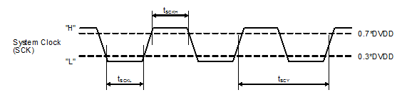 Figure 4. Timing Requirements for SCK Input
7.8 Timing Requirements: PCM Audio Data
| MIN | TYP | MAX | UNIT | ||
|---|---|---|---|---|---|
| tBCY | BCK Pulse Cycle Time | 40 | ns | ||
| tBCL | BCK Pulse Width LOW | 16 | ns | ||
| tBCH | BCK Pulse Width HIGH | 16 | ns | ||
| tBL | BCK Rising Edge to LRCK Edge | 8 | ns | ||
| tBCK | BCK frequency at DVDD = 3.3V | 24.576 | MHz | ||
| tBCK(1.8V) | BCK frequency at DVDD = 1.8V | 12.288 | MHz | ||
| tLB | LRCK Edge to BCK Rising Edge | 8 | ns | ||
| tDS | DATA Set Up Time | 8 | ns | ||
| tDH | DATA Hold Time | 8 | ns | ||
| tDOD | DATA delay time from BCK falling edge | 15 | ns | ||
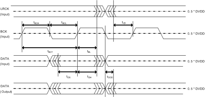 Figure 5. PCM5242 Serial Audio Timing - Slave
In software mode, the PCM5242 can act as an I2S master, generating BCK and LRCK as outputs from the SCK input.
Table 3. I2S Master Mode Registers
| Register | Function |
|---|---|
| Page0, Register 9, D(0), D(4), and D(5) | I2S Master mode select |
| Register 32, D(6:0) | BCK divider and LRCK divider |
| Register 33, D(7:0) |
The I2S master timing is shown in Figure 6.
| MIN | TYP | MAX | UNIT | ||
|---|---|---|---|---|---|
| tBCY | BCK Pulse Cycle Time | 40 | ns | ||
| tBCL | BCK Pulse Width LOW | 16 | ns | ||
| tBCH | BCK Pulse Width HIGH | 16 | ns | ||
| tBCK | BCK frequency at DVDD = 3.3V | 24.576 | MHz | ||
| tBCK(1.8V) | BCK frequency at DVDD = 1.8V | 12.288 | MHz | ||
| tLRD | LRCKx delay time from BCKx falling edge | –10 | 20 | ns | |
| tDS | DATA Set Up Time | 8 | ns | ||
| tDH | DATA Hold Time | 8 | ns | ||
| tDOD | DATA delay time from BCK falling edge at DVDD = 3.3V | 15 | ns | ||
| tDOD(1.8V) | DATA delay time from BCK falling edge at DVDD = 1.8V | 20 | ns | ||
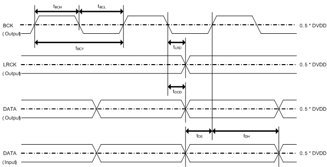 Figure 6. PCM5242 Serial Audio Timing - Master
7.9 Timing Requirements: XSMT
| MIN | TYP | MAX | UNIT | ||
|---|---|---|---|---|---|
| tr | Rise time | 20 | ns | ||
| tf | Fall time | 20 | ns | ||
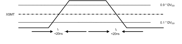 Figure 7. XSMT Timing for Soft Mute and Soft Un-Mute
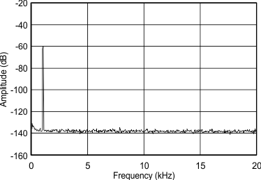
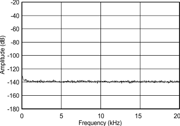
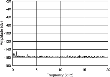
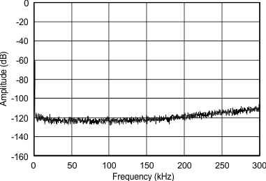
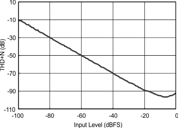
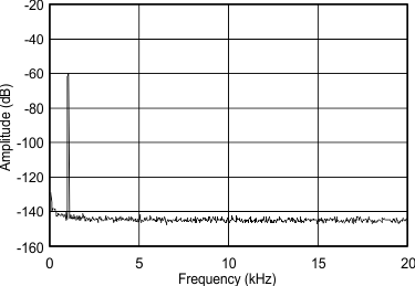
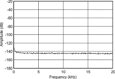
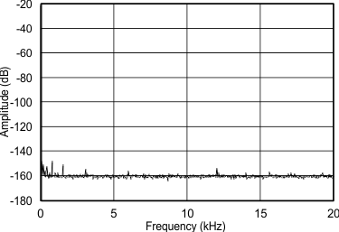
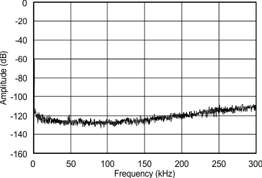
Typical Characteristics
All specifications at TA = 25°C, AVDD = CPVDD = DVDD = 3.3V, fS = 48kHz, system clock = 512 fS and 24-bit data unless otherwise noted.