SBOSA80 December   2021 REF20-Q1

PRODUCTION DATA  

  1. Features
  2. Applications
  3. Description
  4. Revision History
  5. Device Comparison Table
  6. Pin Configuration and Functions
  7. Specifications
    1. 7.1 Absolute Maximum Ratings
    2. 7.2 ESD Ratings
    3. 7.3 Recommended Operating Conditions
    4. 7.4 Thermal Information
    5. 7.5 Electrical Characteristics
    6. 7.6 Typical Characteristics
  8. Parameter Measurement Information
    1. 8.1 Solder Heat Shift
    2. 8.2 Long-Term Stability
    3. 8.3 Thermal Hysteresis
    4. 8.4 Noise Performance
  9. Detailed Description
    1. 9.1 Overview
    2. 9.2 Functional Block Diagram
    3. 9.3 Feature Description
      1. 9.3.1 VREF and VBIAS Tracking
      2. 9.3.2 Low Temperature Drift
      3. 9.3.3 Load Current
    4. 9.4 Device Functional Modes
  10. 10Applications and Implementation
    1. 10.1 Application Information
    2. 10.2 Typical Application
      1. 10.2.1 Low-Side, Current-Sensing Application
        1. 10.2.1.1 Design Requirements
        2. 10.2.1.2 Detailed Design Procedure
          1. 10.2.1.2.1 Shunt Resistor
          2. 10.2.1.2.2 Differential Amplifier
          3. 10.2.1.2.3 Voltage Reference
          4. 10.2.1.2.4 Error Calculations
          5. 10.2.1.2.5 Application Curves
  11. 11Power-Supply Recommendations
  12. 12Layout
    1. 12.1 Layout Guidelines
    2. 12.2 Layout Example
  13. 13Device and Documentation Support
    1. 13.1 Documentation Support
      1. 13.1.1 Related Documentation
    2. 13.2 Receiving Notification of Documentation Updates
    3. 13.3 Support Resources
    4. 13.4 Trademarks
    5. 13.5 Electrostatic Discharge Caution
    6. 13.6 Glossary
  14. 14Mechanical, Packaging, and Orderable Information

Package Options

Mechanical Data (Package|Pins)
Thermal pad, mechanical data (Package|Pins)
Orderable Information

Load Current

The REF20xx-Q1 family is specified to deliver a current load of ±20 mA per output. Both the VREF and VBIAS outputs of the device are protected from short circuits by limiting the output short-circuit current to 50 mA. The device temperature increases according to Equation 4:
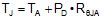
Equation 4. GUID-A5D869E1-8BA8-4706-9C83-92681C3D3F39-low.gif

where

  • TJ = junction temperature (°C)
  • TA = ambient temperature (°C)
  • PD = power dissipated (W)
  • RθJA = junction-to-ambient thermal resistance (°C/W)

The REF20xx-Q1 maximum junction temperature must not exceed the absolute maximum rating of 150°C.