SBVS046D December 2003 – March 2016 REF3112 , REF3120 , REF3125 , REF3130 , REF3133 , REF3140
PRODUCTION DATA.
- 1 Features
- 2 Applications
- 3 Description
- 4 Revision History
- 5 Device Comparison Table
- 6 Pin Configuration and Functions
- 7 Specifications
- 8 Detailed Description
- 9 Application and Implementation
- 10Power Supply Recommendations
- 11Layout
- 12Device and Documentation Support
- 13Mechanical, Packaging, and Orderable Information
Package Options
Refer to the PDF data sheet for device specific package drawings
Mechanical Data (Package|Pins)
- DBZ|3
Thermal pad, mechanical data (Package|Pins)
Orderable Information
9 Application and Implementation
NOTE
Information in the following applications sections is not part of the TI component specification, and TI does not warrant its accuracy or completeness. TI’s customers are responsible for determining suitability of components for their purposes. Customers should validate and test their design implementation to confirm system functionality.
9.1 Application Information
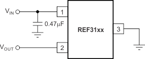
The REF31xx does not require a load capacitor and is stable with any capacitive load. Figure 28 shows typical connections required for operation of the REF31xx. TI recommends a supply bypass capacitor of 0.47 μF.
 Figure 28. Typical Connections for Operating REF31xx
9.2 Typical Application
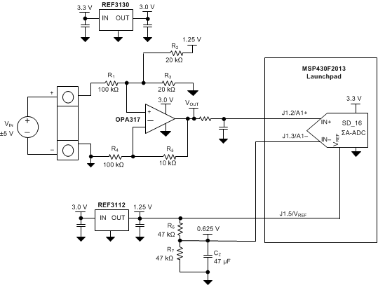
Figure 29 shows a low-power reference and conditioning circuit. This circuit attenuates and level-shifts a bipolar input voltage within the proper input range of a single-supply, low-power, 16-bit ΔΣ ADC, such as the one inside the MSP430 or other similar single-supply ADCs. Precision reference circuits are used to level-shift the input signal, provide the ADC reference voltage, and to create a well-regulated supply voltage for the low-power analog circuitry. A low-power, zero-drift, op-amp circuit is used to attenuate and level-shift the input signal.
 Figure 29. Low-Power Reference and Bipolar Voltage Conditioning Circuit for Low-Power ADCs
9.2.1 Design Requirements
- Supply Voltage: 3.3 V
- Maximum Input Voltage: ±6 V
- Specified Input Voltage: ±5 V
- ADC Reference Voltage: 1.25 V
The goal for this design is to accurately condition a ±5-V bipolar input voltage into a voltage suitable for conversion by a low-voltage ADC with a 1.25-V reference voltage, VREF, and an input voltage range of VREF / 2. The circuit should function with reduced performance over a wider input range of at least ±6 V to allow for easier protection of overvoltage conditions.
9.2.2 Detailed Design Procedure
Figure 29 depicts a simplified schematic for this design showing the MSP430 ADC inputs and full input conditioning circuitry. The ADC is configured for a bipolar measurement where final conversion result is the differential voltage between the voltage at the positive and negative ADC inputs. The bipolar, GND-referenced input signal must be level-shifted and attenuated by the op amp so that the output is biased to VREF/2 and has a differential voltage that is within the ±VREF/2 input range of the ADC.
9.2.3 Application Curves
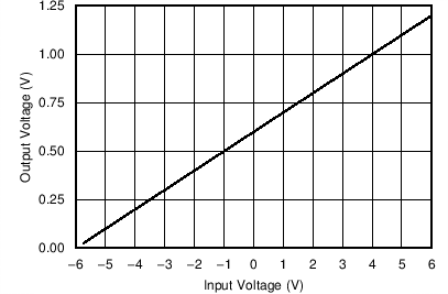
 Figure 30. OPA317 Output Voltage vs Input Voltage
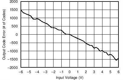
 Figure 32. Output Code Error vs Input Voltage
 Figure 31. OPA317 Output Voltage Error vs Input Voltage