SBOS456H September 2008 – February 2015 REF5020A-Q1 , REF5025A-Q1 , REF5030A-Q1 , REF5040A-Q1 , REF5045A-Q1 , REF5050A-Q1
PRODUCTION DATA.
- 1 Features
- 2 Applications
- 3 Description
- 4 Simplified Schematic
- 5 Revision History
- 6 Pin Configuration and Functions
- 7 Specifications
- 8 Detailed Description
- 9 Application and Implementation
- 10Power Supply Recommendations
- 11Layout
- 12Device and Documentation Support
- 13Mechanical, Packaging, and Orderable Information
Package Options
Mechanical Data (Package|Pins)
- D|8
Thermal pad, mechanical data (Package|Pins)
Orderable Information
8 Detailed Description
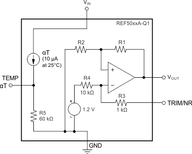
8.1 Overview
The REF50xxA-Q1 family of devices is a low-noise, precision-bandgap voltage reference that is specifically designed for excellent initial voltage accuracy and drift. See the Functional Block Diagram section for a simplified block diagram of the REF50xxA-Q1 family of devices.
8.2 Functional Block Diagram
8.3 Feature Description
8.3.1 Supply Voltage
The REF50xxA-Q1 family of voltage references features extremely low dropout voltage. With the exception of the REF5020A-Q1 device, which has a minimum supply requirement of 2.7 V, these references can operate with a supply of 200 mV above the output voltage in an unloaded condition. For loaded conditions, Figure 6 in the Typical Characteristics section shows a typical dropout voltage versus load plot.
8.3.2 Using the TRIM/NR Pin
The REF50xxA-Q1 family of devices provides a very accurate voltage output. However, VOUT can be adjusted to reduce noise and shift the output voltage from the nominal value by configuring the trim and noise reduction pin (TRIM/NR, pin 5). The TRIM/NR pin provides a ±15-mV adjustment of the device bandgap, which produces a ±15-mV change on the VOUT pin. Figure 25 shows a typical circuit using the TRIM/NR pin to adjust VOUT. When using this technique, the temperature coefficients of the resistors can degrade the temperature drift at the output.
 Figure 25. VOUT Adjustment Using TRIM/NR Pin
The REF50xxA-Q1 family of devices allows access to the bandgap through the TRIM/NR pin. Placing a capacitor from the TRIM/NR pin to GND (as shown in Figure 26) in combination with the internal 1-kΩ resistor creates a low-pass filter that lowers the overall noise measured on the VOUT pin. A capacitance of 1 μF is suggested for a low-pass filter with a corner frequency of 14.5 Hz. Higher capacitance results in a lower cutoff frequency.
 Figure 26. Noise Reduction Using TRIM/NR Pin
8.3.3 Temperature Drift
The REF50xxA-Q1 family of devices is designed for minimal drift error, which is defined as the change in output voltage over temperature. The drift is calculated using the box method. Use Equation 1 to calculate the drift.
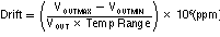
The REF50xxA-Q1 family of devices features a maximum drift coefficient of 8 ppm/°C for the standard-grade.
8.3.4 Temperature Monitoring
The temperature output pin (TEMP, pin 3) provides a temperature-dependent voltage output with approximately 60-kΩ source impedance. As shown in Figure 8, the output voltage follows the nominal relationship:
This pin indicates general chip temperature, accurate to approximately ±15°C. Although this pin is not generally suitable for accurate temperature measurements, it can be used to indicate temperature changes or for temperature compensation of analog circuitry. A temperature change of 30°C corresponds to an approximate 79-mV change in voltage at the TEMP pin.
The TEMP pin has high output impedance (see the Functional Block Diagram section). Loading this pin with a low-impedance circuit induces a measurement error; however, it does not have any effect on VOUT accuracy.
To avoid errors caused by low-impedance loading, buffer the TEMP pin output with a suitable low-temperature drift op amp, such as the OPA333, OPA335, or OPA376, as shown in Figure 27.

8.4 Device Functional Modes
The REF50xxA-Q1 family of devices can only operate in an on or off mode. As long as a sufficient input supply voltage is made available to device, the device performs in standard operation. The device cannot be placed in a low power or shutdown mode.