SBOS456H September 2008 – February 2015 REF5020A-Q1 , REF5025A-Q1 , REF5030A-Q1 , REF5040A-Q1 , REF5045A-Q1 , REF5050A-Q1
PRODUCTION DATA.
- 1 Features
- 2 Applications
- 3 Description
- 4 Simplified Schematic
- 5 Revision History
- 6 Pin Configuration and Functions
- 7 Specifications
- 8 Detailed Description
- 9 Application and Implementation
- 10Power Supply Recommendations
- 11Layout
- 12Device and Documentation Support
- 13Mechanical, Packaging, and Orderable Information
Package Options
Mechanical Data (Package|Pins)
- D|8
Thermal pad, mechanical data (Package|Pins)
Orderable Information
9 Application and Implementation
NOTE
Information in the following applications sections is not part of the TI component specification, and TI does not warrant its accuracy or completeness. TI’s customers are responsible for determining suitability of components for their purposes. Customers should validate and test their design implementation to confirm system functionality.
9.1 Application Information
9.1.1 Thermal Hysteresis
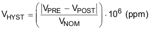
Thermal hysteresis for the REF50xxA-Q1 family of devices is defined as the change in output voltage after operating the device at 25°C, cycling the device through the specified temperature range, and returning to 25°C. Use Equation 3 to calculate the thermal hysteresis.
where
- VHYST = thermal hysteresis (in units of ppm)
- VNOM = the specified output voltage
- VPRE = output voltage measured at 25°C pretemperature cycling
- VPOST = output voltage measured after the device has been cycled from 25°C through the specified temperature range of –40°C to +125°C and returned to 25°C
9.2 Typical Applications
9.2.1 Standalone Applications
Figure 28 shows the typical connections for the REF50xxA-Q1 family of devices.
 Figure 28. Basic Connections
9.2.1.1 Design Requirements
A supply bypass capacitor with a value between 1 μF to 10 μF is recommended. A 1-μF to 50-μF, low-ESR output capacitor (CL) must be connected from VOUT to GND. The ESR value should be less than or equal to 1.5 Ω. The ESR minimizes gain peaking of the internal 1.2-V reference and thus reduces noise at the VOUT pin.
9.2.1.2 Detailed Design Procedure
9.2.1.2.1 Power Dissipation
The REF50xxA-Q1 family of devices is specified to deliver current loads of ±10 mA over the specified input voltage range. The temperature of the device increases according Equation 4.
where
- TJ = Junction temperature (°C)
- TA = Ambient temperature (°C)
- PD = Power dissipated (W)
- RθJA = Junction-to-ambient thermal resistance (°C/W)
The junction temperature of the REF50xxA-Q1 family of devices must not exceed the absolute maximum rating of 150°C.
9.2.1.2.2 Noise Performance
The Electrical Characteristics: Per Device section specifies the typical voltage noise at 0.1 Hz to 10 Hz for each member of the REF50xxA-Q1 family of devices. The noise voltage increases with output voltage and operating temperature. Additional filtering can be used to improve output noise levels, although care should be taken to ensure the output impedance does not degrade performance.
For additional information about how to minimize noise and maximize performance in mixed-signal applications, such as data converters, refer to the series of Analog Applications Journal articles entitled, How a Voltage Reference Affects ADC Performance. See the Related Documentation section for a list of these articles.
9.2.1.3 Application Curves
 Figure 29. Transient Behavior of VOUT
 Figure 30. DC Analysis of VOUT Across Various Temperatures and the Full Output-Current Range
9.2.2 Negative-Reference Voltage Applications
For applications requiring a negative and positive reference voltage, the REF50xxA-Q1 family of devices and the OPA735 device can be used to provide a dual-supply reference from a 5-V supply. Figure 31 shows the REF5025A-Q1 used to provide a 2.5-V supply reference voltage. The low drift performance of the REF50xxA-Q1 family of devices complements the low offset voltage and zero drift of the OPA735 device to provide an accurate solution for split-supply applications. Care must be taken to match the temperature coefficients of R1 and R2.

NOTE:
Bypass capacitors not shown.9.2.3 Data-Acquisition Applications
Data acquisition systems often require stable voltage references to maintain accuracy. The REF50xxA-Q1 family of devices features low noise, very low drift, and high initial accuracy for high-performance data converters. Figure 32 shows the REF5040A-Q1 in a basic data acquisition system.
 Figure 32. Basic Data Acquisition System