SBOS456H September   2008  – February 2015 REF5020A-Q1 , REF5025A-Q1 , REF5030A-Q1 , REF5040A-Q1 , REF5045A-Q1 , REF5050A-Q1

PRODUCTION DATA.  

  1. Features
  2. Applications
  3. Description
  4. Simplified Schematic
  5. Revision History
  6. Pin Configuration and Functions
  7. Specifications
    1. 7.1 Absolute Maximum Ratings
    2. 7.2 ESD Ratings
    3. 7.3 Recommended Operating Conditions
    4. 7.4 Thermal Information
    5. 7.5 Electrical Characteristics: Per Device
    6. 7.6 Electrical Characteristics: All Devices
    7. 7.7 Typical Characteristics
  8. Detailed Description
    1. 8.1 Overview
    2. 8.2 Functional Block Diagram
    3. 8.3 Feature Description
      1. 8.3.1 Supply Voltage
      2. 8.3.2 Using the TRIM/NR Pin
      3. 8.3.3 Temperature Drift
      4. 8.3.4 Temperature Monitoring
    4. 8.4 Device Functional Modes
  9. Application and Implementation
    1. 9.1 Application Information
      1. 9.1.1 Thermal Hysteresis
    2. 9.2 Typical Applications
      1. 9.2.1 Standalone Applications
        1. 9.2.1.1 Design Requirements
        2. 9.2.1.2 Detailed Design Procedure
          1. 9.2.1.2.1 Power Dissipation
          2. 9.2.1.2.2 Noise Performance
        3. 9.2.1.3 Application Curves
      2. 9.2.2 Negative-Reference Voltage Applications
      3. 9.2.3 Data-Acquisition Applications
  10. 10Power Supply Recommendations
  11. 11Layout
    1. 11.1 Layout Guidelines
    2. 11.2 Layout Example
  12. 12Device and Documentation Support
    1. 12.1 Documentation Support
      1. 12.1.1 Related Documentation
    2. 12.2 Related Links
    3. 12.3 Trademarks
    4. 12.4 Electrostatic Discharge Caution
    5. 12.5 Glossary
  13. 13Mechanical, Packaging, and Orderable Information

Package Options

Mechanical Data (Package|Pins)
Thermal pad, mechanical data (Package|Pins)
Orderable Information

6 Pin Configuration and Functions

D Package
8-Pin SOIC
Top View
REF5020A-Q1 REF5025A-Q1 REF5030A-Q1 REF5040A-Q1 REF5045A-Q1 REF5050A-Q1 po_8_soic_sbos456.gif
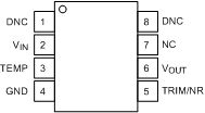
DNC = Do not connect
NC = No internal connection

Pin Functions

PIN I/O DESCRIPTION
NAME NO.
DNC 1 Do not connect. Do not use.
8
GND 4 Ground
NC 7 No internal connection. Do not use.
TEMP 3 O Temperature-dependent voltage output
TRIM/NR 5 I Trim and noise reduction for ±15-mV output adjustment
VIN 2 I Input supply voltage
VOUT 6 O Reference voltage output