SBAS221H December 2001 – October 2015 REG71050 , REG71055
PRODUCTION DATA.
- 1 Features
- 2 Applications
- 3 Description
- 4 Revision History
- 5 Device Comparison Table
- 6 Pin Configuration and Functions
- 7 Specifications
- 8 Detailed Description
- 9 Application and Implementation
- 10Power Supply Recommendations
- 11Layout
- 12Device and Documentation Support
- 13Mechanical, Packaging, and Orderable Information
Package Options
Mechanical Data (Package|Pins)
- DDC|6
Thermal pad, mechanical data (Package|Pins)
Orderable Information
7 Specifications
7.1 Absolute Maximum Ratings
over operating free-air temperature range (unless otherwise noted)| MIN | MAX | UNIT | ||
|---|---|---|---|---|
| VIN | Supply voltage | –0.3 | 6 | V |
| Enable | Enable input | –0.3 | VIN | |
| Output short-circuit duration | Indefinite | |||
| TA | Operating ambient temperature | –55 | 125 | °C |
| TJ | Operating ambient temperature | –55 | 150 | |
| Tstg | Storage temperature | –55 | 150 | |
7.2 ESD Ratings
| VALUE | UNIT | |||
|---|---|---|---|---|
| V(ESD) | Electrostatic discharge | Human body model (HBM), per ANSI/ESDA/JEDEC JS-001(1) | ±2000 | V |
| Charged device model (CDM), per JEDEC specification JESD22-C101(2) | ±500 | |||
(1) JEDEC document JEP155 states that 500-V HBM allows safe manufacturing with a standard ESD control process.
(2) JEDEC document JEP157 states that 250-V CDM allows safe manufacturing with a standard ESD control process.
7.3 Recommended Operating Conditions
over operating free-air temperature range (unless otherwise noted)| MIN | NOM | MAX | UNIT | |||
|---|---|---|---|---|---|---|
| INPUT VOLTAGE | ||||||
| Tested Startup(1) | REG71055 | 3 | 5.5 | V | ||
| REG710-5 | 2.7 | 5.5 | V | |||
| All other models | 1.8 | 5.5 | V | |||
| TA | Operating ambient temperature range | –40 | 85 | °C | ||
(1) See conditions under Output Voltage with a resistive load no lower than typical VOUT/IOUT in Electrical Characteristics.
7.4 Thermal Information
| THERMAL METRIC(1) | REG710 | UNIT | |||
|---|---|---|---|---|---|
| DRV | DDC | DBV | |||
| 6 PINS | 6 PINS | 6 PINS | |||
| RθJA | Junction-to-ambient thermal resistance | 119.1 | 204.6 | 184.4 | °C/W |
| RθJC(top) | Junction-to-case (top) thermal resistance | 110.5 | 50.5 | 124.6 | °C/W |
| RθJB | Junction-to-board thermal resistance | 88.7 | 54.3 | 30.6 | °C/W |
| ψJT | Junction-to-top characterization parameter | 7.7 | 0.8 | 22.1 | °C/W |
| ψJB | Junction-to-board characterization parameter | 89 | 52.8 | 30.1 | °C/W |
| RθJC(bot) | Junction-to-case (bottom) thermal resistance | 61.8 | n/a | n/a | °C/W |
(1) For more information about traditional and new thermal metrics, see the Semiconductor and IC Package Thermal Metrics application report, SPRA953.
7.5 Electrical Characteristics
TA = -40ºC to 85ºC, typical values are at TA = 25°C (unless otherwise noted), VIN = (VOUT / 2 + 0.75 V), IOUT = 10 mA, CIN = COUT = 2.2 μF, CPUMP = 0.22 μF, and VENABLE = 1.3 V, unless otherwise noted.| PARAMETER | TEST CONDITIONS | MIN | TYP | MAX | UNIT | |||
|---|---|---|---|---|---|---|---|---|
| SUPPLY | ||||||||
| VIN | Input voltage range. Tested Startup. | See conditions under Output Voltage with a resistive load no lower than typical VOUT/IOUT. |
||||||
| REG71055 | 3 | 5.5 | V | |||||
| REG710-5 | 2.7 | 5.5 | ||||||
| All other models | 1.8 | 5.5 | ||||||
| IQ | Operating quiescent current | IOUT = 0 mA, TA = 25°C | 65 | 100 | μA | |||
| ISD | Shutdown current | VIN = 1.8 V to 5.5 V, Enable = 0 V, TA = 25°C | 0.01 | 1 | μA | |||
| CONTROL SIGNALS (ENABLE) | ||||||||
| Logic high input voltage | VIN = 1.8 V to 5.5 V | 1.3 | VIN | V | ||||
| Logic low input voltage | VIN = 1.8 V to 5.5 V | –0.2 | 0.4 | V | ||||
| Logic high input current | VIN = 1.8 V to 5.5 V, TA = 25°C | 100 | nA | |||||
| Logic low input current | VIN = 1.8 V to 5.5 V, TA = 25°C | 100 | nA | |||||
| OSCILLATOR FREQUENCY(1) | 1 | MHz | ||||||
| OUTPUT | ||||||||
| REG71055 | IOUT ≤ 10 mA, 3 V ≤ VIN ≤ 5.5 V | 5.2 | 5.5 | 5.8 | V | |||
| IOUT ≤ 30 mA, 3.25 V ≤ VIN ≤ 5.5 V | 5.2 | 5.5 | 5.8 | V | ||||
| REG710-5, REG71050 | IOUT ≤ 10 mA, 2.7 V ≤ VIN ≤ 5.5 V | 4.7 | 5 | 5.3 | V | |||
| IOUT ≤ 30 mA, 3 V ≤ VIN ≤ 5.5 V | 4.7 | 5 | 5.3 | V | ||||
| IOUT ≤ 60 mA, 3.3 V ≤ VIN ≤ 4.2 V | 4.6 | 5 | 5.4 | V | ||||
| REG710-3.3 | IOUT ≤ 10 mA, 1.8 V ≤ VIN ≤ 5.5 V | 3.1 | 3.3 | 3.5 | V | |||
| IOUT ≤ 30 mA, 2.2 V ≤ VIN ≤ 5.5 V | 3.1 | 3.3 | 3.5 | V | ||||
| REG710-3 | IOUT ≤ 10 mA, 1.8 V ≤ VIN ≤ 5.5 V | 2.82 | 3 | 3.18 | V | |||
| IOUT ≤ 30 mA, 2.2 V ≤ VIN ≤ 5.5 V | 2.82 | 3 | 3.18 | V | ||||
| REG710-2.7 | IOUT ≤ 10 mA, 1.8 V ≤ VIN ≤ 5.5 V | 2.54 | 2.7 | 2.86 | V | |||
| IOUT ≤ 30 mA, 2 V ≤ VIN ≤ 5.5 V | 2.54 | 2.7 | 2.86 | V | ||||
| REG710-2.5 | IOUT ≤ 10 mA, 1.8 V ≤ VIN ≤ 5.5 V | 2.35 | 2.5 | 2.65 | V | |||
| IOUT ≤ 30 mA, 2 V ≤ VIN ≤ 5.5 V | 2.35 | 2.5 | 2.65 | V | ||||
| Iout | Nominal output current | TA = 25°C | 30 | mA | ||||
| Isc | Short circuit output current | TA = 25°C | 100 | mA | ||||
| RIPPLE VOLTAGE (3) | IOUT = 30 mA, TA = 25°C | 35 | mVPP | |||||
| EFFICIENCY(2) | IOUT = 10 mA, VIN = 1.8 V, REG710-3.3, TA = 25°C | 90% | ||||||
| THERMAL SHUTDOWN | ||||||||
| Shutdown temperature | 160 | °C | ||||||
| Shutdown recovery | 140 | °C | ||||||
(1) The converter regulates by enabling and disabling periods of switching cycles. The switching frequency is the oscillator frequency during an active period.
(2) See efficiency curves for other VIN/VOUT configurations.
(3) Effective series resistance (ESR) of capacitors is < 0.1 Ω.
7.6 Typical Characteristics
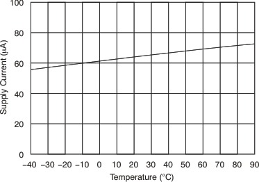
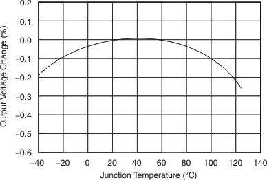
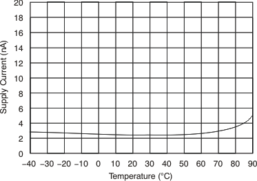
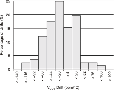
At TA = 25°C, VIN = (VOUT / 2 + 0.75 V), IOUT = 5 mA, CIN = COUT = 2.2 μF, CPUMP = 0.22 μF, and VENABLE = 1.3 V, unless otherwise noted.
| No load | ||


| Not enabled | ||
