SPNS180B September 2012 – June 2015 RM42L432
PRODUCTION DATA.
- 1Device Overview
- 2Revision History
- 3Device Comparison
-
4Terminal Configuration and Functions
- 4.1 PZ QFP Package Pinout (100-Pin)
- 4.2
Terminal Functions
- 4.2.1 High-End Timer (N2HET)
- 4.2.2 Enhanced Quadrature Encoder Pulse Modules (eQEP)
- 4.2.3 General-Purpose Input/Output (GPIO)
- 4.2.4 Controller Area Network Interface Modules (DCAN1, DCAN2)
- 4.2.5 Multibuffered Serial Peripheral Interface (MibSPI1)
- 4.2.6 Standard Serial Peripheral Interface (SPI2)
- 4.2.7 Local Interconnect Network Controller (LIN)
- 4.2.8 Multibuffered Analog-to-Digital Converter (MibADC)
- 4.2.9 System Module
- 4.2.10 Error Signaling Module (ESM)
- 4.2.11 Main Oscillator
- 4.2.12 Test/Debug Interface
- 4.2.13 Flash
- 4.2.14 Core Supply
- 4.2.15 I/O Supply
- 4.2.16 Core and I/O Supply Ground Reference
- 4.3 Output Multiplexing and Control
- 4.4 Special Multiplexed Options
-
5Specifications
- 5.1 Absolute Maximum Ratings
- 5.2 ESD Ratings
- 5.3 Power-On Hours (POH)
- 5.4 Recommended Operating Conditions
- 5.5 Switching Characteristics Over Recommended Operating Conditions for Clock Domains
- 5.6 Wait States Required
- 5.7 Power Consumption
- 5.8 Thermal Resistance Characteristics for PZ
- 5.9 Input/Output Electrical Characteristics
- 5.10 Output Buffer Drive Strengths
- 5.11 Input Timings
- 5.12 Output Timings
-
6System Information and Electrical Specifications
- 6.1 Voltage Monitor Characteristics
- 6.2 Power Sequencing and Power-On Reset
- 6.3 Warm Reset (nRST)
- 6.4 ARM Cortex-R4 CPU Information
- 6.5 Clocks
- 6.6 Clock Monitoring
- 6.7 Glitch Filters
- 6.8 Device Memory Map
- 6.9 Flash Memory
- 6.10 Flash Program and Erase Timings for Program Flash
- 6.11 Flash Program and Erase Timings for Data Flash
- 6.12 Tightly Coupled RAM Interface Module
- 6.13 Parity Protection for Accesses to peripheral RAMs
- 6.14 On-Chip SRAM Initialization and Testing
- 6.15 Vectored Interrupt Manager
- 6.16 Real-Time Interrupt Module
- 6.17 Error Signaling Module
- 6.18 Reset / Abort / Error Sources
- 6.19 Digital Windowed Watchdog
- 6.20 Debug Subsystem
-
7Peripheral Information and Electrical Specifications
- 7.1 Peripheral Legend
- 7.2 Multibuffered 12-Bit Analog-to-Digital Converter
- 7.3 General-Purpose Input/Output
- 7.4 Enhanced High-End Timer (N2HET)
- 7.5 Controller Area Network (DCAN)
- 7.6 Local Interconnect Network Interface (LIN)
- 7.7 Multibuffered / Standard Serial Peripheral Interface
- 7.8 Enhanced Quadrature Encoder (eQEP)
- 8Device and Documentation Support
- 9Mechanical Packaging and Orderable Addendum
Package Options
Refer to the PDF data sheet for device specific package drawings
Mechanical Data (Package|Pins)
- PZ|100
Thermal pad, mechanical data (Package|Pins)
Orderable Information
8 Device and Documentation Support
8.1 Device Support
8.1.1 Development Support
Texas Instruments (TI) offers an extensive line of development tools for the Hercules™ Safety generation of MCUs, including tools to evaluate the performance of the processors, generate code, develop algorithm implementations, and fully integrate and debug software and hardware modules.
The following products support development of Hercules™-based applications:
Software Development Tools
- Code Composer Studio™ Integrated Development Environment (IDE)
- C/C++ Compiler
- Code generation tools
- Assembler/Linker
- Cycle Accurate Simulator
- Application algorithms
- Sample applications code
Hardware Development Tools
- Development and evaluation boards
- JTAG-based emulators - XDS100™v2, XDS200, XDS560™ v2 emulator
- Flash programming tools
- Power supply
- Documentation and cables
8.1.1.1 Getting Started
This section gives a brief overview of the steps to take when first developing for a RM4x MCU device. For more detail on each of these steps, see the following:
8.1.2 Device Nomenclature
To designate the stages in the product development cycle, TI assigns prefixes to the part numbers of all devices.Each device has one of three prefixes: X, P, or null (no prefix) (for example, xRM46L852). These prefixes represent evolutionary stages of product development from engineering prototypes through fully qualified production devices/tools.
Device development evolutionary flow:
-
x Experimental device that is not necessarily representative of the final device's electrical specifications and may not use production assembly flow.
-
P Prototype device that is not necessarily the final silicon die and may not necessarily meet final electrical specifications.
-
null Fully-qualified production device.
x and P devices and TMDX development-support tools are shipped against the following disclaimer:
"Developmental product is intended for internal evaluation purposes."
Production devices have been characterized fully, and the quality and reliability of the device have been demonstrated fully. TI's standard warranty applies.
Predictions show that prototype devices have a greater failure rate than the standard production devices. Texas Instruments recommends that these devices not be used in any production system because their expected end-use failure rate still is undefined. Only qualified production devices are to be used.
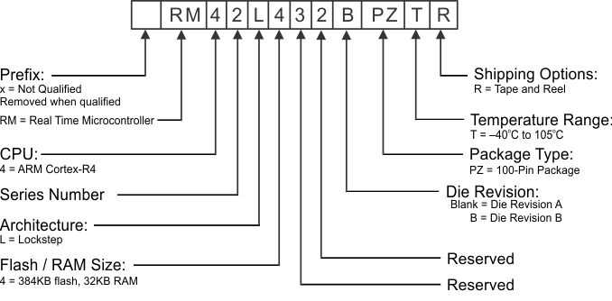
Figure 8-1 illustrates the numbering and symbol nomenclature for the RM42L432.
8.2 Documentation Support
8.2.1 Related Documentation from Texas Instruments
The following documents describe the RM42L432 microcontroller.
-
SPNU516RM42L42x 16/32-Bit RISC Flash Microcontroller Technical Reference Manual details the integration, the environment, the functional description, and the programming models for each peripheral and subsystem in the device.
-
SPNZ198RM42L432 Microcontroller, Silicon Revision A, Silicon Errata describes the usage notes and known exceptions to the functional specifications for the device silicon revision(s).
-
SPNZ227RM42x Microcontroller, Silicon Revision B, Silicon Errata describes the usage notes and known exceptions to the functional specifications for the device silicon revision(s).
-
SPNA207Calculating Equivalent Power-on-Hours for Hercules™ Safety MCUs details how to use the spreadsheet to calculate the aging effect of temperature on Texas Instruments Hercules Safety MCUs.
8.3 Community Resources
The following links connect to TI community resources. Linked contents are provided "AS IS" by the respective contributors. They do not constitute TI specifications and do not necessarily reflect TI's views; see TI's Terms of Use.
-
TI E2E™ Online Community TI's Engineer-to-Engineer (E2E) Community. Created to foster collaboration among engineers. At e2e.ti.com, you can ask questions, share knowledge, explore ideas and help solve problems with fellow engineers.
-
TI Embedded Processors Wiki Texas Instruments Embedded Processors Wiki. Established to help developers get started with Embedded Processors from Texas Instruments and to foster innovation and growth of general knowledge about the hardware and software surrounding these devices.
8.4 Trademarks
Hercules, Code Composer Studio, XDS100, XDS560, E2E are trademarks of Texas Instruments.
ARM, Cortex are registered trademarks of ARM Limited (or its subsidiaries) in the EU and.
CoreSight is a trademark of ARM Limited.
All other trademarks are the property of their respective owners.
8.5 Electrostatic Discharge Caution

This integrated circuit can be damaged by ESD. Texas Instruments recommends that all integrated circuits be handled with appropriate precautions. Failure to observe proper handling and installation procedures can cause damage.
ESD damage can range from subtle performance degradation to complete device failure. Precision integrated circuits may be more susceptible to damage because very small parametric changes could cause the device not to meet its published specifications.
8.6 Glossary
SLYZ022 — TI Glossary.
This glossary lists and explains terms, acronyms, and definitions.
8.7 Device Identification Code Register
The device identification code register identifies several aspects of the device including the silicon version. The details of the device identification code register are shown in Table 8-1. The device identification code register value for this device is:
| 31 | 30 | 29 | 28 | 27 | 26 | 25 | 24 | 23 | 22 | 21 | 20 | 19 | 18 | 17 | 16 |
| CP-15 | UNIQUE ID | TECH | |||||||||||||
| R-1 | R-00000000100100 | R-0 | |||||||||||||
| 15 | 14 | 13 | 12 | 11 | 10 | 9 | 8 | 7 | 6 | 5 | 4 | 3 | 2 | 1 | 0 |
| TECH | I/O VOLTAGE | PERIPH PARITY | FLASH ECC | RAM ECC | VERSION | 1 | 0 | 1 | |||||||
| R-101 | R-0 | R-1 | R-10 | R-1 | R-00001 | R-1 | R-0 | R-1 | |||||||
| LEGEND: R/W = Read/Write; R = Read only; -n = value after reset |
Table 8-1 Device ID Bit Allocation Register Field Descriptions
| BIT | FIELD | VALUE | DESCRIPTION |
|---|---|---|---|
| 31 | CP15 | Indicates the presence of coprocessor 15 | |
| 1 | CP15 present | ||
| 30-17 | UNIQUE ID | 100100 |
Silicon version (revision) bits. This bit field holds a unique number for a dedicated device configuration (die). |
| 16-13 | TECH | Process technology on which the device is manufactured. | |
| 0101 | F021 | ||
| 12 | I/O VOLTAGE | I/O voltage of the device. | |
| 0 | I/O are 3.3v | ||
| 11 | PERIPHERAL PARITY | Peripheral Parity | |
| 1 | Parity on peripheral memories | ||
| 10-9 | FLASH ECC | Flash ECC | |
| 10 | Program memory with ECC | ||
| 8 | RAM ECC | Indicates if RAM memory ECC is present. | |
| 1 | ECC implemented | ||
| 7-3 | REVISION | 0 | Revision of the Device. |
| 2-0 | FAMILY ID | 101 | The platform family ID is always 0b101 |
8.8 Die Identification Registers
The two die ID registers at addresses 0xFFFFFF7C and 0xFFFFFF80 form a 64-bit die id with the information as shown in Table 8-2.
Table 8-2 Die-ID Registers
| ITEM | NO. OF BITS | BIT LOCATION |
|---|---|---|
| X Coord. on Wafer | 12 | 0xFFFFFF7C[11:0] |
| Y Coord. on Wafer | 12 | 0xFFFFFF7C[23:12] |
| Wafer # | 8 | 0xFFFFFF7C[31:24] |
| Lot # | 24 | 0xFFFFFF80[23:0] |
| Reserved | 8 | 0xFFFFFF80[31:24] |
8.9 Module Certifications
The following communications modules have received certification of adherence to a standard.
8.9.1 DCAN Certification
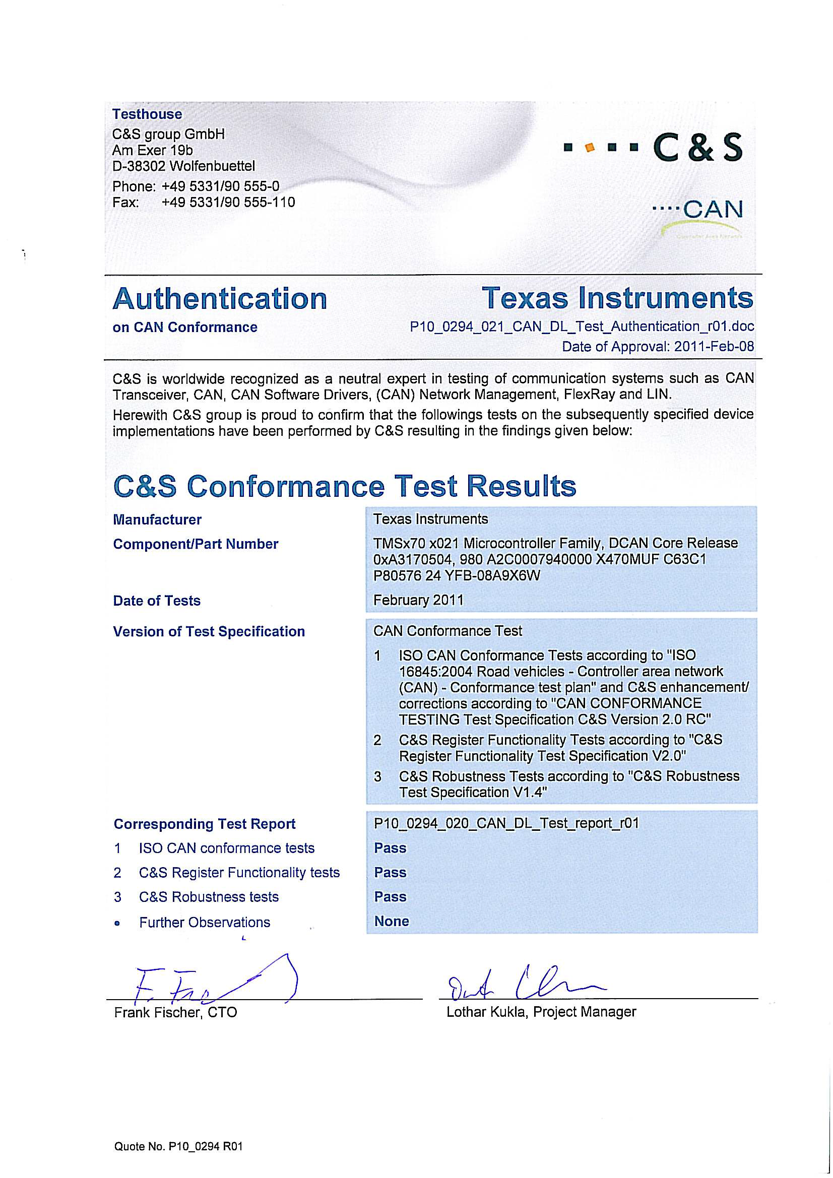 Figure 8-3 DCAN Certification
8.9.2 LIN Certifications
8.9.2.1 LIN Master Mode
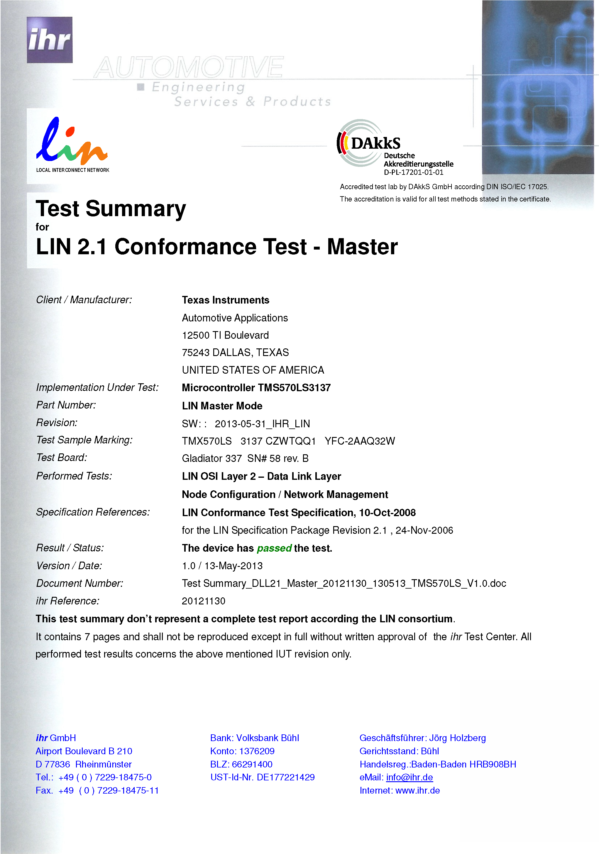 Figure 8-4 LIN Certification - Master Mode
8.9.2.2 LIN Slave Mode - Fixed Baud Rate
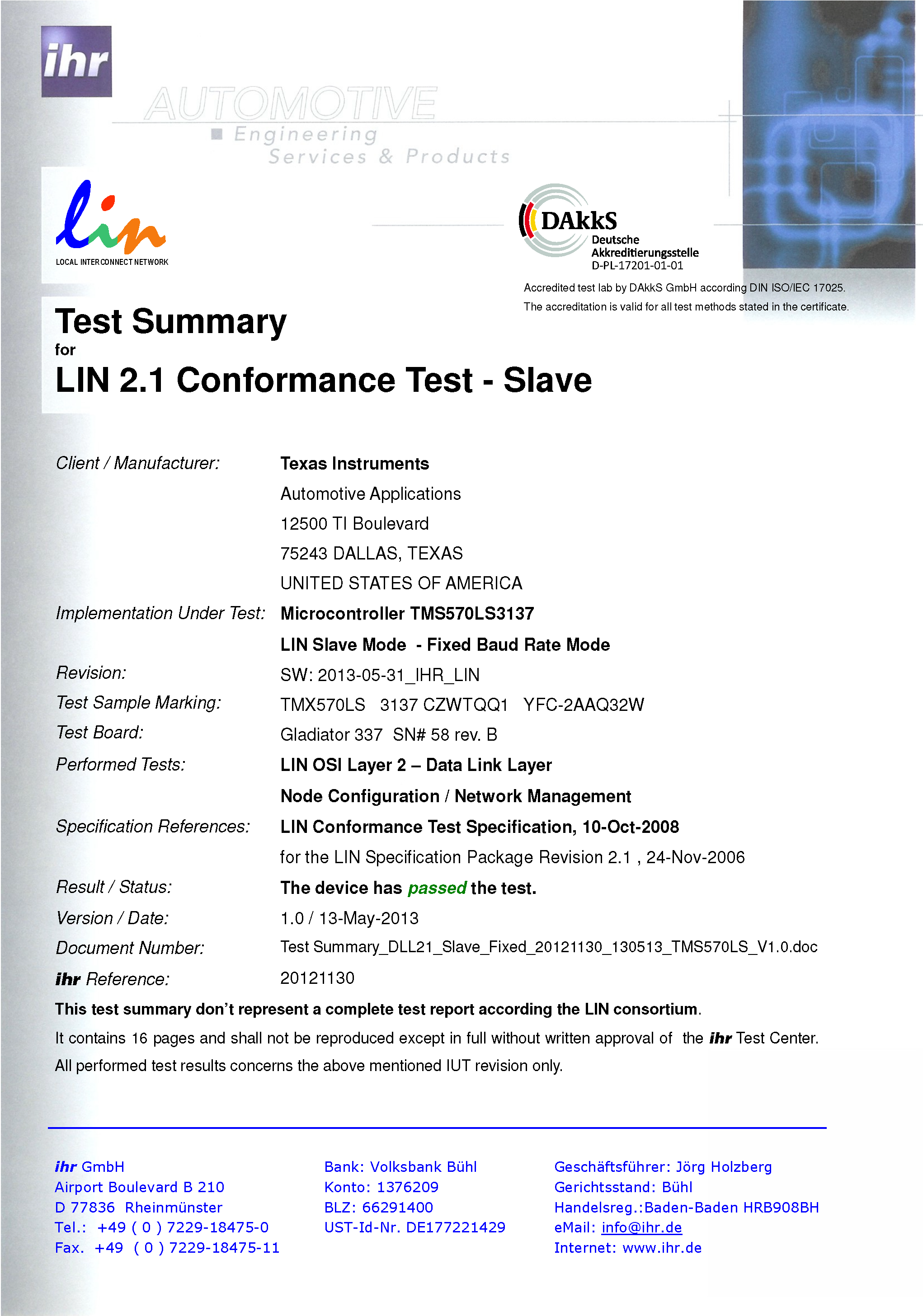 Figure 8-5 LIN Certification - Slave Mode - Fixed Baud Rate
8.9.2.3 LIN Slave Mode - Adaptive Baud Rate
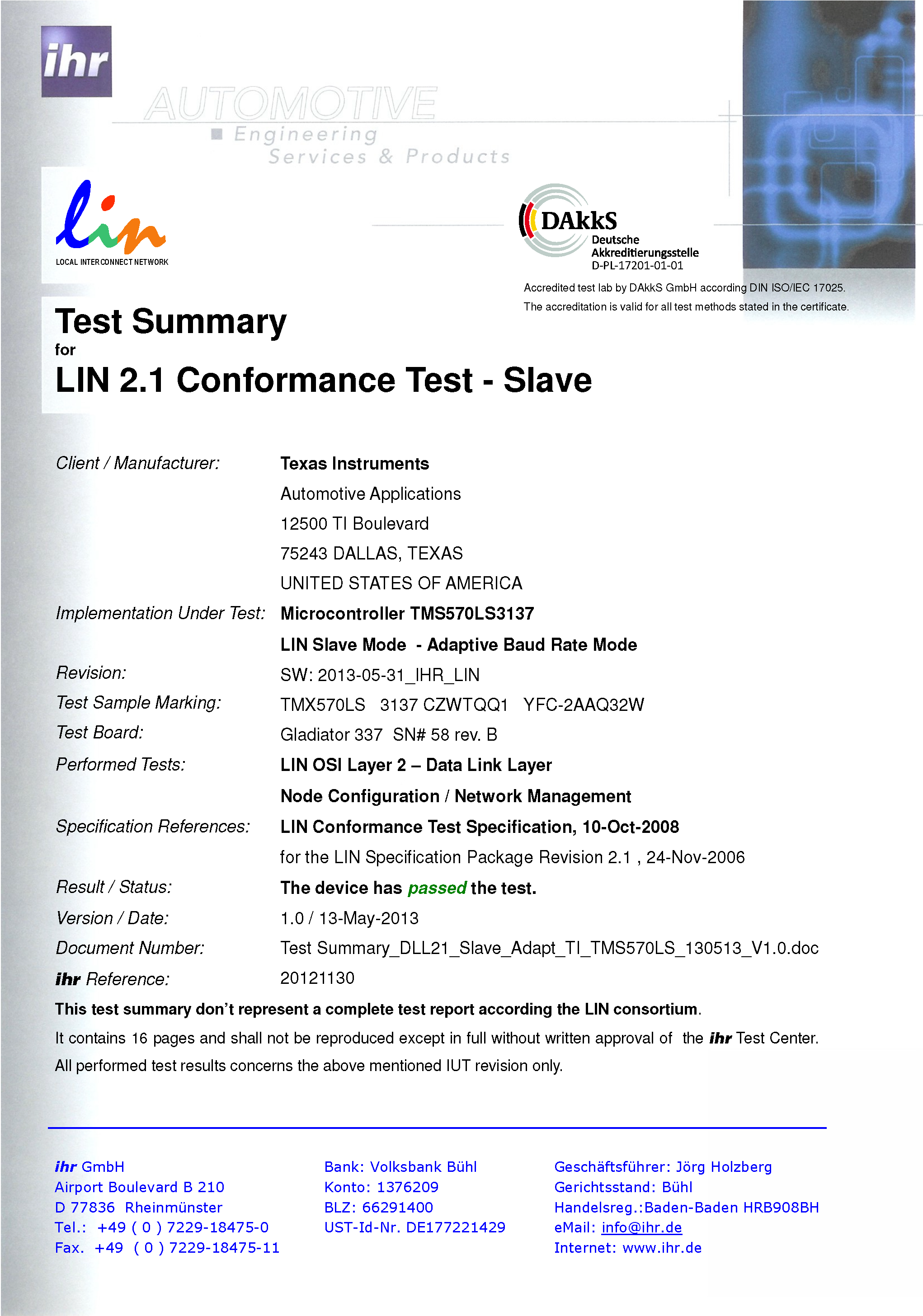 Figure 8-6 LIN Certification - Slave Mode - Adaptive Baud Rate
