SNOSBA2B July 2011 – May 2015 SM74101
PRODUCTION DATA.
- 1 Features
- 2 Applications
- 3 Description
- 4 Revision History
- 5 Pin Configuration and Functions
- 6 Specifications
- 7 Detailed Description
- 8 Application and Implementation
- 9 Power Supply Recommendations
- 10Layout
- 11Device and Documentation Support
- 12Mechanical, Packaging, and Orderable Information
Package Options
Mechanical Data (Package|Pins)
- NGG|6
Thermal pad, mechanical data (Package|Pins)
Orderable Information
10 Layout
10.1 Layout Guidelines
Attention must be given to board layout when using the SM74101. Proper grounding is crucial. The driver needs a very low impedance path for current return to ground avoiding inductive loops. Two paths for returning current to ground are a) between SM74101 IN_REF pin and the ground of the circuit that controls the driver inputs and b) between SM74101 VEE pin and the source of the power MOSFET being driven. Both paths should be as short as possible to reduce inductance and be as wide as possible to reduce resistance. These ground paths should be distinctly separate to avoid coupling between the high current paths (VCC, VEE, and OUT) and the logic signal paths (IN, INB, and IN_REF) of the SM74101. With rise and fall times in the range of 10 to 30 ns, care is required to minimize the lengths of current carrying conductors to reduce their inductance and EMI from the high di/dt transients generated when driving large capacitive loads.
10.2 Layout Example
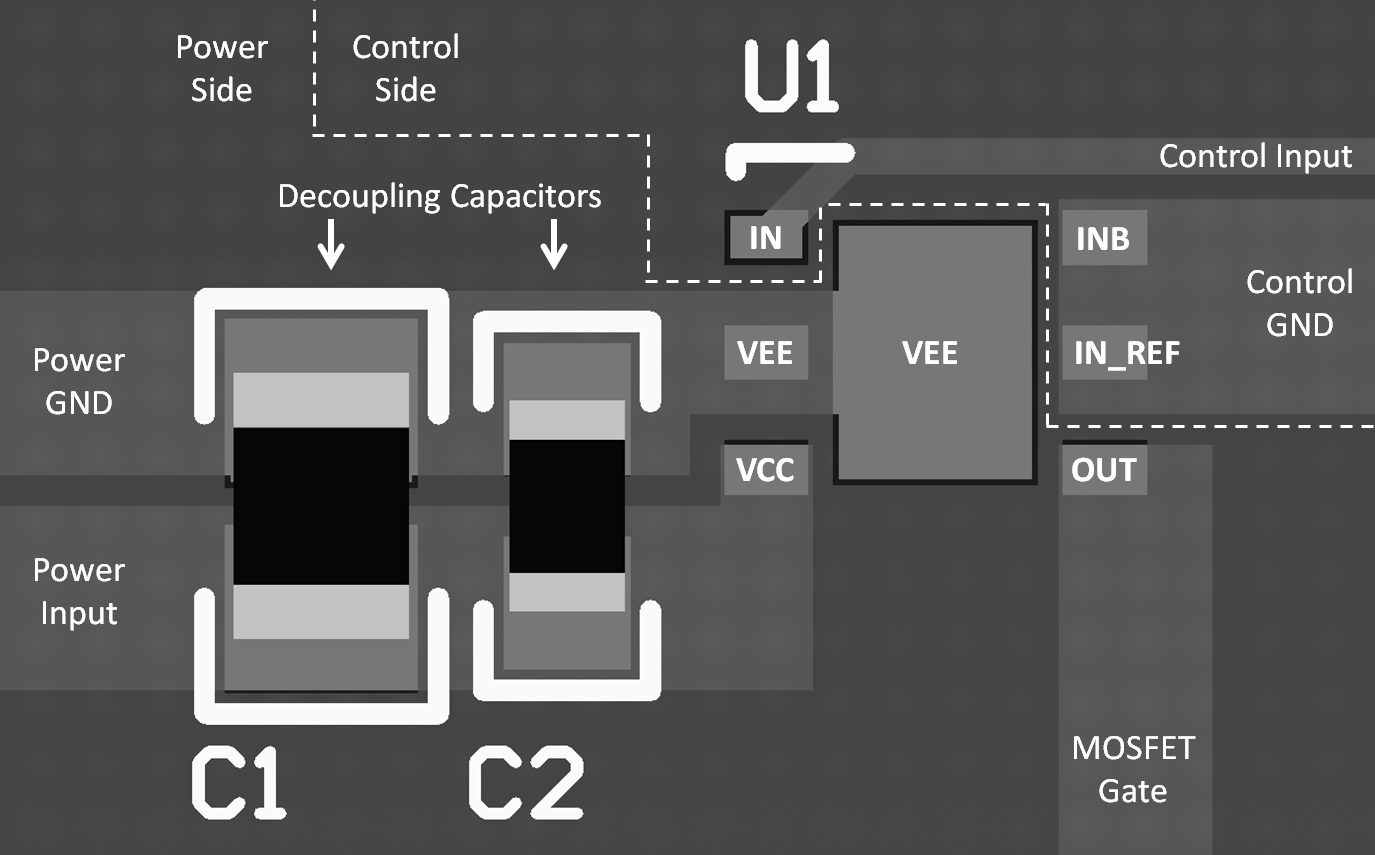
Figure 16 shows an example layout for the SM74101 configured in the non-inverting mode of operation. In this mode, the INB pin is not used and is connected to IN_REF. Two low ESR/ESL capacitors, C1 and C2, are used for input decoupling purposes and are placed as close as possible to the IC.
The level shift circuit and the separate input/output ground pins provide the option of single supply or split supply configurations. When driving the MOSFET gate from a single positive supply, the control ground should be connected to the power ground in an area of the board where the least amount of noise will exist. Otherwise, when using a split supply configuration, the control ground and power ground paths should be distinctly separate to avoid noise coupling between the two paths.
 Figure 16. SM74101 Layout Example