SCLS470C March 2003 – June 2022 SN54HC109 , SN74HC109
PRODUCTION DATA
- 1 Features
- 2 Description
- 3 Revision History
- 4 Pin Configuration and Functions
- 5 Specifications
- 6 Parameter Measurement Information
- 7 Detailed Description
- 8 Power Supply Recommendations
- 9 Layout
- 10Device and Documentation Support
- 11Mechanical, Packaging, and Orderable Information
Package Options
Refer to the PDF data sheet for device specific package drawings
Mechanical Data (Package|Pins)
- W|16
Thermal pad, mechanical data (Package|Pins)
Orderable Information
2 Description
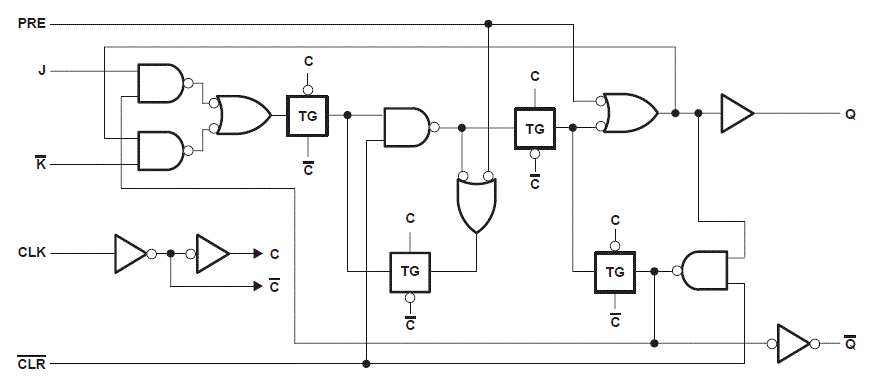
These devices contain two independent J-K positive-edge-triggered flip-flops. A low level at the preset (PRE) or clear (CLR) inputs sets or resets the outputs, regardless of the levels of the other inputs. When PRE and CLR are inactive (high), data at the J and K inputs meeting the setup-time requirements are transferred to the outputs on the positive-going edge of the clock (CLK) pulse. Clock triggering occurs at a voltage level and is not related directly to the rise time of the clock pulse. Following the hold-time interval, data at the J and K inputs can be changed without affecting the levels at the outputs. These versatile flip-flops can perform as toggle flip-flops by grounding K and tying J high. They also can perform as D-type flip-flops if J and K are tied together.
| PART NUMBER | PACKAGE(1) | BODY SIZE (NOM) |
|---|---|---|
| SN54HC109J | CDIP (16) | 24.38 mm × 6.92 mm |
| SN74HC109D | SOIC (16) | 9.90 mm × 3.90 mm |
| SN74HC109N | PDIP (16) | 19.31 mm × 6.35 mm |
| SN74HC109NS | SO (16) | 6.20 mm × 5.30 mm |
| SNJ54HC109FK | LCCC (20) | 8.89 mm × 8.45 mm |
| SNJ54HC109W | CFP (16) | 10.16 mm × 6.73 mm |
 Functional Block Diagram