SCLS041J December 1982 – October 2021 SN54HC595 , SN74HC595
PRODUCTION DATA
- 1 Features
- 2 Applications
- 3 Description
- 4 Revision History
- 5 Pin Configuration and Functions
- 6 Specifications
- 7 Parameter Measurement Information
- 8 Detailed Description
- 9 Application and Implementation
- 10Power Supply Recommendations
- 11Layout
- 12Device and Documentation Support
- 13Mechanical, Packaging, and Orderable Information
Package Options
Mechanical Data (Package|Pins)
Thermal pad, mechanical data (Package|Pins)
Orderable Information
3 Description
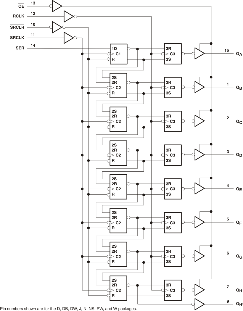
The SNx4HC595 devices contain an 8-bit, serial-in, parallel-out shift register that feeds an 8-bit D-type storage register. The storage register has parallel 3-state outputs. Separate clocks are provided for both the shift and storage register. The shift register has a direct overriding clear (SRCLR) input, serial (SER) input, and serial outputs for cascading. When the output-enable (OE) input is high, the outputs are in the high-impedance state.
Device Information
| PART NUMBER | PACKAGE(1) | BODY SIZE (NOM) |
|---|---|---|
| SN54HC595FK | LCCC (20) | 8.89 mm × 8.89 mm |
| SN54HC595J | CDIP (16) | 21.34 mm × 6.92 mm |
| SN74HC595N | PDIP (16) | 19.31 mm × 6.35 mm |
| SN74HC595D | SOIC (16) | 9.90 mm × 3.90 mm |
| SN74HC595DW | SOIC (16) | 10.30 mm × 7.50 mm |
| SN74HC595DB | SSOP (16) | 6.20 mm × 5.30 mm |
| SN74HC595PW | TSSOP (16) | 5.00 mm × 4.40 mm |
(1) For all available packages, see the orderable addendum at the end of the data sheet.
 Functional Block
Diagram