SCLS010F December 1982 – May 2022 SN54HC688 , SN74HC688
PRODUCTION DATA
- 1 Features
- 2 Description
- 3 Revision History
- 4 Pin Configuration and Functions
- 5 Specifications
- 6 Parameter Measurement Information
- 7 Detailed Description
- 8 Power Supply Recommendations
- 9 Layout
- 10Device and Documentation Support
- 11Mechanical, Packaging, and Orderable Information
Package Options
Refer to the PDF data sheet for device specific package drawings
Mechanical Data (Package|Pins)
- J|20
- FK|20
Thermal pad, mechanical data (Package|Pins)
Orderable Information
2 Description
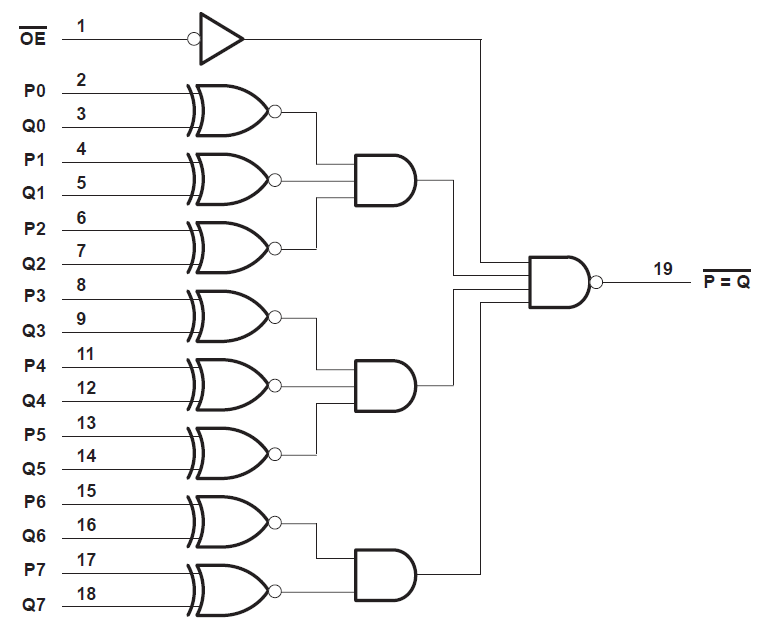
These identity comparators perform comparisons of two 8-bit binary or BCD words. An output-enable (OE) input may be used to force the output to the high level.
Device
Information
| PART NUMBER | PACKAGE(1) | BODY SIZE (NOM) |
|---|---|---|
| SN74HC688DW | SOIC (20) | 12.80 mm × 7.50 mm |
| SN74HC688N | PDIP (20) | 25.40 mm × 6.35 mm |
| SN74HC688PWR | TSSOP (20) | 6.50 mm × 4.40 mm |
| SN54HC688J | CDIP (20) | 26.92 mm × 6.92 mm |
| SNJ54HC688FK | LCCC (20) | 8.89 mm × 8.45 mm |
(1) For all available packages, see the orderable
addendum at the end of the data sheet.
 Functional Block Diagram