SDLS146B October 1976 – September 2016 SN54LS245 , SN74LS245
- 1 Features
- 2 Applications
- 3 Description
- 4 Revision History
- 5 Device Comparison Table
- 6 Pin Configuration and Functions
- 7 Specifications
- 8 Parameter Measurement Information
- 9 Detailed Description
- 10Application and Implementation
- 11Power Supply Recommendations
- 12Layout
- 13Device and Documentation Support
- 14Mechanical, Packaging, and Orderable Information
Package Options
Refer to the PDF data sheet for device specific package drawings
Mechanical Data (Package|Pins)
- W|20
- J|20
- FK|20
Thermal pad, mechanical data (Package|Pins)
Orderable Information
10 Application and Implementation
NOTE
Information in the following applications sections is not part of the TI component specification, and TI does not warrant its accuracy or completeness. TI’s customers are responsible for determining suitability of components for their purposes. Customers should validate and test their design implementation to confirm system functionality.
10.1 Application Information
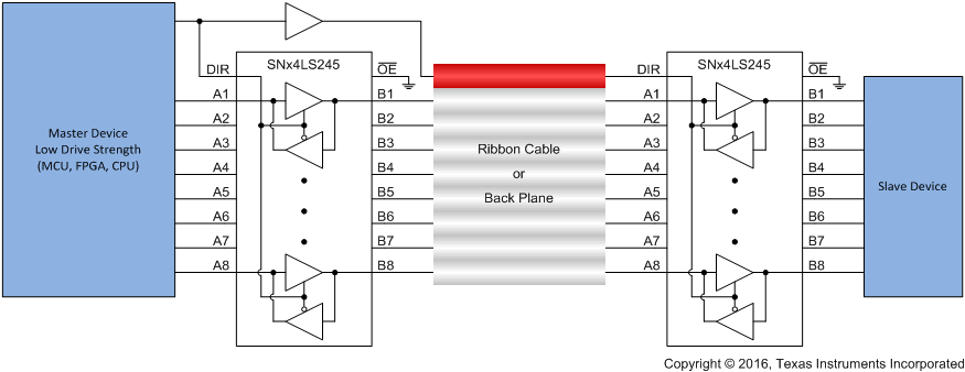
The SNx4LS245 is commonly used to drive ribbon cables or back plane busses. It allows isolation from the bus when necessary, and increases drive strength on the bus.
10.2 Typical Application
Figure 5 shows the SNx4LS245 wired up as a permanently enabled data bus transceiver for both a master and slave device communicating over a ribbon cable or back plane.
 Figure 5. SNx4LS245 Being Used to Communicate Over a Ribbon Cable or Back Plane
10.2.1 Design Requirements
This device uses Schottky transistor logic technology. Take care to avoid bus contention because it can drive currents that would exceed maximum limits. The high drive creates fast edges into light loads, so routing and load conditions must be considered to prevent ringing.
10.2.2 Detailed Design Procedure
- Power Supply
- Each device must maintain a supply voltage between 4.5 V and 5.5 V
- Inputs
- Input signals must meet the VIH and VIL specifications in Electrical Characteristics
- Inputs leakage values (II, IIH, IIL) from Electrical Characteristics must be considered
- Outputs
- Output signals are specified to meet the VOH and VOL specifications in Electrical Characteristics as a minimum (the values could be closer to VCC for high signals or GND for low signals)
- TI recommends maintaining output currents as specified in Recommended Operating Conditions
- The part can be damaged by sourcing or sinking too much current. See Electrical Characteristics for details.
10.2.3 Application Curve
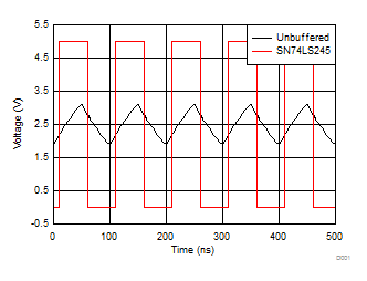
It is common to see significant losses in ribbon cables and back planes. Figure 6 shows a simplified simulation of a ribbon cable from a 5-V, 10-MHz low-drive strength source. It shows the difference between an input signal from a weak driver like an MCU or FPGA compared to a strong driver like the SN74LS245 when measured at the distant end of the cable. By adding a high-current drive transceiver before the cable, the signal strength can be significantly improved, and subsequently the cable can be longer.
