SCAS990 March 2024 SN54SC8T138-SEP
ADVANCE INFORMATION
- 1
- 1 Features
- 2 Applications
- 3 Description
- 4 Pin Configuration and Functions
- 5 Specifications
- 6 Parameter Measurement Information
- 7 Detailed Description
- 8 Application and Implementation
- 9 Device and Documentation Support
- 10Revision History
- 11Mechanical, Packaging, and Orderable Information
Package Options
Refer to the PDF data sheet for device specific package drawings
Mechanical Data (Package|Pins)
- PW|16
Thermal pad, mechanical data (Package|Pins)
Orderable Information
3 Description
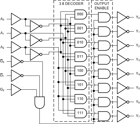
The SN54SC8T138-SEP is a three to eight decoder with one standard output strobe (G2) and two active low output strobes (G1 and G0). When the outputs are gated by any of the strobe inputs, they are all forced into the high state. When the outputs are not disabled by the strobe inputs, only the selected output is low while all others are high. The output level is referenced to the supply voltage (VCC) and supports 1.8-V, 2.5-V, 3.3-V, and 5-V CMOS levels.
The input is designed with a lower threshold circuit to support up translation for lower voltage CMOS inputs (for example, 1.2 V input to 1.8 V output or 1.8 V input to 3.3 V output). In addition, the 5-V tolerant input pins enable down translation (for example, 3.3 V to 2.5 V output).
| PART NUMBER | PACKAGE(1) | PACKAGE SIZE(2) | BODY SIZE (NOM)(3) |
|---|---|---|---|
| SN54SC8T138-SEP | PW (TSSOP, 16) | 5 mm × 6.4 mm | 5 mm × 4.4 mm |
 Simplified Logic Diagram (Positive Logic)