SLLSEI2A September 2017 – December 2017 SN55HVD233-SP
PRODUCTION DATA.
- 1 Features
- 2 Applications
- 3 Description
- 4 Revision History
- 5 Description (continued)
- 6 Pin Configuration and Functions
-
7 Specifications
- 7.1 Absolute Maximum Ratings
- 7.2 ESD Ratings
- 7.3 Recommended Operating Conditions
- 7.4 Thermal Information
- 7.5 Driver Electrical Characteristics
- 7.6 Receiver Electrical Characteristics
- 7.7 Driver Switching Characteristics
- 7.8 Receiver Switching Characteristics
- 7.9 Device Switching Characteristics
- 7.10 Typical Characteristics
- 8 Parameter Measurement Information
- 9 Detailed Description
- 10Application and Implementation
- 11Power Supply Recommendations
- 12Layout
- 13Device and Documentation Support
- 14Mechanical, Packaging, and Orderable Information
Package Options
Refer to the PDF data sheet for device specific package drawings
Mechanical Data (Package|Pins)
- HKX|8
Thermal pad, mechanical data (Package|Pins)
Orderable Information
9 Detailed Description
9.1 Overview
The SN55HVD233-SP is used in applications employing the CAN serial communication physical layer in accordance with the ISO 11898 standard. As a CAN transceiver, the device provides transmit and receive capability between the differential CAN bus and a CAN controller, with signaling rates up to 1 Mbps.
Designed for operation in especially harsh environments, the SN55HVD233-SP features cross-wire, overvoltage, and loss of ground protection to ±16 V, overtemperature (thermal shutdown) protection, and common-mode transient protection of ±100 V. This device operates over a wide –7-V to 12-V common mode range. This transceiver is the interface between the host CAN controller on the microprocessor, FPGA, or ASIC, and the differential CAN bus used in satellite applications.
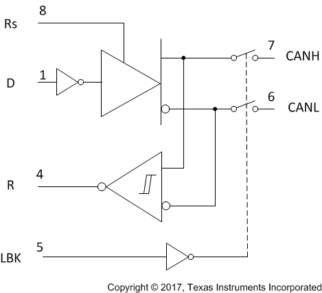
9.2 Functional Block Diagram

9.3 Feature Description
9.3.1 Modes
The RS, pin 8 of the SN55HVD233-SP, provides for three modes of operation: high-speed, slope control, or low-power standby mode. The user selects the high-speed mode of operation by connecting pin 8 directly to ground, allowing the driver output transistors to switch on and off as fast as possible with no limitation on the rise and fall slope. The user can adjust the rise and fall slope by connecting a resistor to ground at pin 8, because the slope is proportional to the pin's output current. Slope control is implemented with a resistor values of 0 Ω to achieve a single ended slew rate of approximately 38 V/μs up to a value of 50 kΩ to achieve approximately 4 V/μs slew rate. For more information about slope control, refer to Application and Implementation.
The SN55HVD233-SP enters a low-current standby (listen-only) mode during which the driver is switched off and the receiver remains active if a high logic level is applied to pin 8. The local protocol controller reverses this low-current standby mode when it needs to transmit to the bus.
9.3.2 Loopback
A logic high on the loopback LBK pin 5 of the SN55HVD233-SP places the bus output and bus input in a high-impedance state. The remaining circuit remains active and available for driver-to-receiver loopback, self-diagnostic node functions without disturbing the bus. For more information on the loopback mode, refer to the Application Information.
9.3.3 CAN Bus States
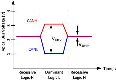
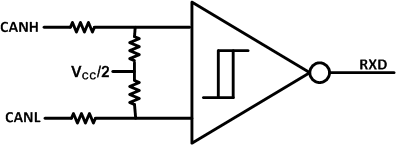
The CAN bus has two states during powered operation of the device: dominant and recessive. A dominant bus state is when the bus is driven differentially, corresponding to a logic low on the D and R pin. A recessive bus state is when the bus is biased to VCC / 2 through the high-resistance internal input resistors RIN of the receiver, corresponding to a logic high on the D and R pins (see Figure 25 and Figure 26).
 Figure 25. Bus States (Physical Bit Representation)
 Figure 26. Simplified Recessive Common Mode Bias and Receiver
9.3.4 ISO 11898 Compliance of SN55HVD233-SP
9.3.4.1 Introduction
Many users value the low-power consumption of operating their CAN transceivers from a 3.3-V supply. However, some users are concerned about the interoperability with 5-V supplied transceivers on the same bus. This report analyzes this situation to address those concerns.
9.3.4.2 Differential Signal
CAN is a differential bus where complementary signals are sent over two wires and the voltage difference between the two wires defines the logical state of the bus. The differential CAN receiver monitors this voltage difference and outputs the bus state with a single-ended output signal.
 Figure 27. Typical SN55HVD233-SP Differential Output Voltage Waveform
The CAN driver creates the difference in voltage between CANH and CANL in the dominant state. The dominant differential output of the SN55HVD233-SP is greater than 1.5 V and less than 3 V across a 60-Ω load. The minimum required by ISO 11898 is 1.5 V and maximum is 3 V. These are the same limiting values for 5-V supplied CAN transceivers. The bus termination resistors drive the recessive bus state and not the CAN driver.
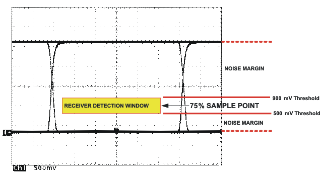
A CAN receiver is required to output a recessive state with less than 500 mV and a dominant state with more than 900 mV difference voltage on its bus inputs. The CAN receiver must do this with common-mode input voltages from –2 V to 7 V. The SN55HVD233-SP receiver meets these same input specifications as 5-V supplied receivers.
9.3.4.2.1 Common-Mode Signal
A common-mode signal is an average voltage of the two signal wires that the differential receiver rejects. The common-mode signal comes from the CAN driver, ground noise, and coupled bus noise. The supply voltage of the CAN transceiver has nothing to do with noise. The SN55HVD233-SP driver lowers the common-mode output in a dominant bit by a couple hundred millivolts from that of most 5-V drivers. While this does not fully comply with ISO 11898, this small variation in the driver common-mode output is rejected by differential receivers and does not effect data, signal noise margins, or error rates.
9.3.4.3 Interoperability of 3.3-V CAN in 5-V CAN Systems
The 3.3-V supplied CAN transceivers are electrically interchangeable with 5-V CAN transceivers. The differential output is the same. The recessive common mode output is the same. The dominant common mode output voltage is a couple hundred millivolts lower than 5 V supplied drivers, while the receivers exhibit identical specifications as 5-V devices.
To help ensure the widest interoperability possible, the SN55HVD233-SP successfully passed the internationally recognized GIFT ICT conformance and interoperability testing for CAN transceivers. Electrical interoperability does not always assure interchangeability, however. Most implementers of CAN buses recognize that ISO 11898 does not sufficiently specify the electrical layer and that strict standard compliance alone does not ensure full interchangeability. Interchangeability is ensured with thorough equipment testing.
9.3.5 Thermal Shutdown
If the junction temperature of the device exceeds the thermal shutdown threshold, the device turns off the CAN driver circuits thus blocking the D pin to bus transmission path. The shutdown condition is cleared when the junction temperature drops below the thermal shutdown temperature of the device. The CAN bus pins are high-impedance biased to recessive level during a thermal shutdown, and the receiver-to-R pin path remains operational.
9.4 Device Functional Modes
Table 3. Driver I/O
| DRIVER(1) | |||||
|---|---|---|---|---|---|
| INPUTS | OUTPUTS | ||||
| D | LBK | RS | CANH | CANL | BUS STATE |
| X | X | > 0.75 VCC | Z | Z | Recessive |
| L | L or open | ≤ 0.33 VCC | H | L | Dominant |
| H or open | X | Z | Z | Recessive | |
| X | H | ≤ 0.33 VCC | Z | Z | Recessive |
Table 4. Receiver I/O
| RECEIVER(1) | ||||
|---|---|---|---|---|
| INPUTS | OUTPUT | |||
| BUS STATE | VID = V(CANH) – V(CANL) | D | R | |
| Dominant | VID ≥ 0.9 V | X | L | |
| Recessive | VID ≤ 0.5 V or open | H or open | H | |
| ? | 0.5 V < VID < 0.9 V | H or open | ? | |
| Dominant | VID ≥ 0.9 V | X | L | |
| Recessive | VID ≤ 0.5 V or open | H | H | |
| Recessive | VID ≤ 0.5 V or open | L | L | |
| ? | 0.5 V < VID < 0.9 V | L | L | |