SLLS545G November 2002 – October 2015 SN55HVD251 , SN65HVD251
PRODUCTION DATA.
- 1 Features
- 2 Applications
- 3 Description
- 4 Revision History
- 5 Pin Configuration and Functions
-
6 Specifications
- 6.1 Absolute Maximum Ratings
- 6.2 ESD Ratings
- 6.3 Recommended Operating Conditions
- 6.4 Thermal Information
- 6.5 Supply Current
- 6.6 Electrical Characteristics: Driver
- 6.7 Electrical Characteristics: Receiver
- 6.8 VREF-Pin Characteristics
- 6.9 Power Dissipation Characteristics
- 6.10 Switching Characteristics: Driver
- 6.11 Switching Characteristics: Device
- 6.12 Switching Characteristics: Receiver
- 6.13 Dissipation Ratings
- 6.14 Typical Characteristics
- 7 Parameter Measurement Information
- 8 Detailed Description
- 9 Application and Implementation
- 10Power Supply Recommendations
- 11Layout
- 12Device and Documentation Support
- 13Mechanical, Packaging, and Orderable Information
Package Options
Mechanical Data (Package|Pins)
- DRJ|8
Thermal pad, mechanical data (Package|Pins)
- DRJ|8
Orderable Information
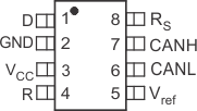
5 Pin Configuration and Functions
D Package
8-Pin SOIC
Top View

Pin Functions
| PIN | I/O | DESCRIPTION | |
|---|---|---|---|
| NAME | NO. | ||
| CANH | 7 | I/O | High-level CAN bus line |
| CANL | 6 | I/O | Low-level CAN bus line |
| D | 1 | I | CAN transmit data input (LOW for dominant and HIGH for recessive bus states), also called TXD, driver input |
| GND | 2 | GND | Ground connection |
| R | 4 | O | CAN receive data output (LOW for dominant and HIGH for recessive bus states), also called RXD, receiver output |
| RS | 8 | I | Mode select pin: strong pulldown to GND = high-speed mode, strong pull up to VCC = low-power mode, 10-kΩ to 100-kΩ pulldown to GND = slope control mode |
| VCC | 3 | Supply | Transceiver 5-V supply voltage |
| VREF | 5 | O | Reference output voltage |