SLLSFI8 February 2021 SN55LVCP22A-SP
PRODUCTION DATA
- 1 Features
- 2 Applications
- 3 Description
- 4 Revision History
- 5 Pin Configuration and Functions
- 6 Specifications
- 7 Parameter Measurement Information
- 8 Detailed Description
- 9 Application and Implementation
- 10Power Supply Recommendations
- 11Layout
- 12Device and Documentation Support
- 13Mechanical, Packaging, and Orderable Information
Package Options
Mechanical Data (Package|Pins)
- W|16
Thermal pad, mechanical data (Package|Pins)
Orderable Information
3 Description
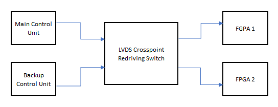
The SN55LVCP22A-SP is a 2×2 crosspoint switch providing greater than 1000 Mbps operation for each path. The dual channels incorporate wide common-mode (0 V to 4 V) receivers, allowing for the receipt of LVDS, LVPECL, and CML signals. The dual outputs are LVDS drivers to provide low-power, low-EMI, high-speed operation. The SN55LVCP22A-SP provides a single device supporting 2:2 buffering (repeating), 1:2 splitting, 2:1 multiplexing, 2×2 switching, and LVPECL/CML to LVDS level translation on each channel. The flexible operation of the SN55LVCP22A-SP provides a single device to support the redundant serial bus transmission needs (working and protection switching cards) of fault-tolerant switch systems found in optical networking, wireless infrastructure, and data communications systems.
The SN55LVCP22A-SP uses a fully differential data path to ensure low-noise generation, fast switching times, low pulse width distortion, and low jitter. Output channel-to- channel skew is 80 ps (typ) to ensure accurate alignment of outputs in all applications.
| PART NUMBER | GRADE | PACKAGE(1) | BODY SIZE (NOM) |
|---|---|---|---|
| 5962R1124201VFA | QMLV RHA | CFP (16) | 6.73 mm x 10.3 mm |
| SN55LVCP22W/EM | Engineering Samples(2) | CFP (16) | 6.73 mm x 10.3 mm |
 Simplified Application