SLLS295B April 1998 – January 2023 SN65ALS1176
PRODUCTION DATA
- 1 Features
- 2 Applications
- 3 Description
- 4 Revision History
- 5 Pin Configuration and Functions
- 6 Specifications
- 7 Parameter Measurement Information
- 8 Detailed Description
- 9 Application and Implementation
- 10Device and Documentation Support
- 11Mechanical, Packaging, and Orderable Information
Package Options
Refer to the PDF data sheet for device specific package drawings
Mechanical Data (Package|Pins)
- D|8
Thermal pad, mechanical data (Package|Pins)
Orderable Information
3 Description
The SN65ALS1176 differential bus transceiver is designed for bidirectional data communication on multipoint bus transmission lines. The device is designed for balanced transmission lines and meets TIA/EIA-422-B, TIA/EIA-485-A, and ITU Recommendations V.11 and X.27.
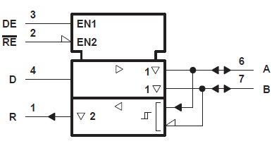
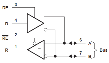
The SN65ALS1176 combines a 3-state differential line driver and a differential input line receiver, both of which operate from a single 5-V power supply. The driver and receiver have active-high and active-low enables, respectively, that can be connected together externally to function as a direction control. The driver differential outputs and the receiver differential inputs are connected internally to form a differential input/output (I/O) bus port that is designed to offer minimum loading to the bus when the driver is disabled or VCC = 0. This port features wide positive and negative common-mode voltage ranges, making the device an excellent choice for party-line applications.
The SN65ALS1176 is characterized for operation from – 25°C to 85°C.
| PART NUMBER | PACKAGE(1) | BODY SIZE (NOM) |
|---|---|---|
| SN65ALS1176 | D (SOIC) | 4.9 mm x 3.91 mm |

 Logic Diagram (Positive Logic)