SLLSEJ5A July 2014 – December 2015 SN65DSI86-Q1
PRODUCTION DATA.
- 1 Features
- 2 Applications
- 3 Description
- 4 Revision History
- 5 Description (continued)
- 6 Pin Configuration and Functions
- 7 Specifications
-
8 Detailed Description
- 8.1 Overview
- 8.2 Functional Block Diagram
- 8.3 Feature Description
- 8.4
Device Functional Modes
- 8.4.1 Reset Implementation
- 8.4.2 Power-Up Sequence
- 8.4.3 Power Down Sequence
- 8.4.4 Display Serial Interface (DSI)
- 8.4.5
DisplayPort
- 8.4.5.1 HPD (Hot Plug/Unplug Detection)
- 8.4.5.2 AUX_CH
- 8.4.5.3 I2C-Over-AUX
- 8.4.5.4 DisplayPort PLL
- 8.4.5.5 DP Output VOD and Pre-emphasis Settings
- 8.4.5.6 DP Main Link Configurability
- 8.4.5.7 DP Main Link Training
- 8.4.5.8 Panel Size vs DP Configuration
- 8.4.5.9 Panel Self Refresh (PSR)
- 8.4.5.10 Secondary Data Packet (SDP)
- 8.4.5.11 Color Bar Generator
- 8.4.5.12 DP Pattern
- 8.4.5.13 BPP Conversion
- 8.5 Programming
- 8.6 Register Map
- 9 Application and Implementation
- 10Power Supply Recommendations
- 11Layout
- 12Device and Documentation Support
- 13Mechanical, Packaging, and Orderable Information
Package Options
Mechanical Data (Package|Pins)
- PAP|64
Thermal pad, mechanical data (Package|Pins)
- PAP|64
Orderable Information
1 Features
- Embedded DisplayPort™ (eDP™) 1.4 Compliant Supporting 1, 2, or 4 Lanes at 1.62 Gbps (RBR), 2.16 Gbps, 2.43 Gbps, 2.7 Gbps (HBR), 3.24 Gbps, 4.32 Gbps, or 5.4 Gbps (HBR2).
- Implements MIPI® D-PHY Version 1.1 Physical Layer Front-End and Display Serial Interface (DSI) Version 1.02.00
- Dual-Channel DSI Receiver Configurable for One, Two, Three, or Four D-PHY Data Lanes Per Channel Operating up to 1.5 Gbps Per Lane
- Supports 18 bpp and 24 bpp DSI Video Packets With RGB666 and RGB888 Formats
- Suitable for 60 fps 4K 4096 × 2304 Resolution at 18 bpp Color, and WUXGA 1920 × 1200 Resolution with 3D Graphics at 60 fps (120 fps Equivalent)
- MIPI Front-End Configurable for Single-Channel or Dual-Channel DSI Configuration
- Supports Dual-Channel DSI Odd, Even and Left, Right Operating Modes
- 1.2-V Main VCC Power Supply and 1.8-V Supply for Digital I/Os
- Low-Power Features Include Panel Refresh and MIPI Ultralow Power State (ULPS) Support
- DisplayPort Lane Polarity and Assignment Configurable.
- Supports 12-MHz, 19.2-MHz, 26-MHz, 27-MHz, and 38.4-MHz Frequencies Through External Reference Clock (REFCLK)
- ESD Rating ±2 kV (HBM)
- Packaged in 64-Terminal HTQFP (PAP)
- Temperature Range: –40°C to +85°C
2 Applications
- Tablet PCs, Notebook PCs, Netbooks
- Mobile Internet Devices/Automotive Infotainment
3 Description
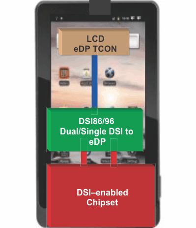
The SN65DSI86-Q1 DSI to embedded DisplayPort (eDP) bridge features a dual-channel MIPI D-PHY receiver front-end configuration with four lanes per channel operating at 1.5 Gbps per lane and a maximum input bandwidth of 12 Gbps. The bridge decodes MIPI DSI 18-bpp RGB666 and 24-bpp RGB888 packets and converts the formatted video data stream to a DisplayPort with up to four lanes at either 1.62 Gbps, 2.16 Gbps, 2.43 Gbps, 2.7 Gbps, 3.24 Gbps, 4.32 Gbps, or 5.4 Gbps.
The SN65DSI86-Q1 is well suited for WQXGA at 60 frames per second, as well as 3D graphics at 4K and true HD (1920 × 1080) resolutions at an equivalent 120 fps with up to 24 bpp. Partial line buffering is implemented to accommodate the data stream mismatch between the DSI and DisplayPort interfaces.
Device Information(1)
| PART NUMBER | PACKAGE | BODY SIZE (NOM) |
|---|---|---|
| SN65DSI86-Q1 | HTQFP (64) | 10 mm x 10 mm |
- For all available packages, see the package option addendum at the end of the datasheet.
