SLLS533F May 2002 – March 2023 SN65HVD05 , SN65HVD06 , SN65HVD07 , SN75HVD06 , SN75HVD07
PRODUCTION DATA
- 1 Features
- 2 Applications
- 3 Description
- 4 Revision History
-
5 Specifications
- 5.1 Absolute Maximum Ratings
- 5.2 Recommended Operating Conditions
- 5.3 Thermal Information
- 5.4 Package Dissipation Ratings
- 5.5 Driver Electrical Characteristics
- 5.6 Driver Switching Characteristics
- 5.7 Receiver Electrical Characteristics
- 5.8 Receiver Switching Characteristics
- 5.9 Typical Characteristics
- 6 Function Tables
- 7 Equivalent Input and Output Schematic Diagrams
- 8 Application and Implementation
- 9 Device and Documentation Support
- 10Mechanical, Packaging, and Orderable Information
Package Options
Mechanical Data (Package|Pins)
Thermal pad, mechanical data (Package|Pins)
Orderable Information
3 Description
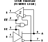
The SN65HVD05, SN75HVD05, SN65HVD06, SN75HVD06, SN65HVD07, and SN75HVD07 combine a 3-state differential line driver and differential line receiver. They are designed for balanced data transmission and interoperate with ANSI TIA/EIA-485-A and ISO 8482E standard-compliant devices. The driver is designed to provide a differential output voltage greater than that required by these standards for increased noise margin. The drivers and receivers have active-high and active-low enables respectively, which can be externally connected together to function as direction control.
The driver differential outputs and receiver differential inputs connect internally to form a differential input/ output (I/O) bus port that is designed to offer minimum loading to the bus whenever the driver is disabled or not powered. These devices feature wide positive and negative common-mode voltage ranges, making them suitable for party-line applications.
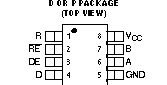
 Figure 3-1 Differential Output
Voltage vs Differential Output Current
Figure 3-1 Differential Output
Voltage vs Differential Output Current