SLLSE84D May 2011 – May 2017 SN65HVD101 , SN65HVD102
PRODUCTION DATA.
- 1 Features
- 2 Applications
- 3 Description
- 4 Revision History
- 5 Device Comparison Table
- 6 Pin Configuration and Functions
- 7 Specifications
- 8 Parameter Measurement
-
9 Detailed Description
- 9.1 Overview
- 9.2 Functional Block Diagram
- 9.3
Feature Description
- 9.3.1 Wake-up Detection
- 9.3.2 Current Limit Indication - Short Circuit Current Detection
- 9.3.3 Active Current Limit Condition: VTHL > VCQ ≥ VTHH
- 9.3.4 Inactive Current Limit Condition: VTHL < VCQ < VTHH
- 9.3.5 Over-temperature Detection
- 9.3.6 CQ Current-limit Adjustment
- 9.3.7 Transceiver Function Tables
- 9.3.8 Voltage Regulator (Not Available in SN65HVD102)
- 9.4 Device Functional Modes
- 10Application and Implementation
- 11Power Supply Recommendations
- 12Layout
- 13Device and Documentation Support
- 14Mechanical, Packaging, and Orderable Information
Package Options
Mechanical Data (Package|Pins)
- RGB|20
Thermal pad, mechanical data (Package|Pins)
- RGB|20
Orderable Information
9 Detailed Description
9.1 Overview
An IO-Link device comprises a transducer or physics to digital converter and the device transceiver (Figure 7). When the device is connected to an IO-Link master through the three-wire interface, the master can initiate communication and exchange data with a remote node with the SN65HVD101 or SN65HVD102 IO-Link transceiver acting as a complete physical layer for the communication.
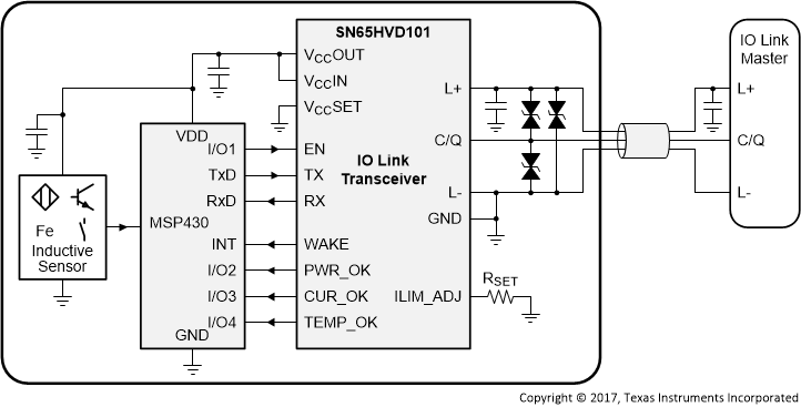 Figure 7. IO-Link Device-to-Master Interface
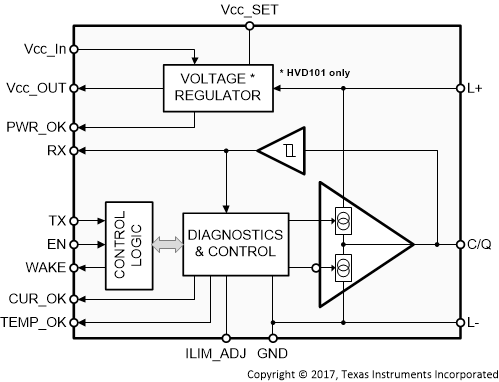
The functional block diagram shows that the device driver output (CQ) can be used in push-pull, high-side, or low-side configurations using the enable (EN) and transmit data (TX) input pins. The internal receiver converts the 24-V IO-Link signal on the CQ line to standard logic levels on the receive data (RX) pin. A simple parallel interface is used to receive and transmit data and status information between the slave and the local controller.
IO-Link transceivers commonly implement protection features for overcurrent, overvoltage and overtemperature conditions. They also provide a current-limit setting of the driver output current using an external resistor. If a short circuit (SC) occurs, the driver outputs are internally limited, and the slave generates an error signal.
The transceiver also possesses an overtemperature shutdown feature that protects the device from high-temperature faults. A modern transceiver can operate either from an external 3.3-V or 5-V low-volt supply, or derives the low-volt supply from the IO-Link L+ voltage (24V nominal) via a linear regulator, to provide power to the local controller and sensor circuitry.
9.2 Functional Block Diagram
9.3 Feature Description
9.3.1 Wake-up Detection
The device may be in IO-Link mode or SIO mode. If the device is in SIO mode and the master node wants to initiate communication with the device node, the master drives the CQ line to the opposite of its present state, and will either sink or source the wake up current (IQWU is typically up to 500 mA) for the wake-up duration (tWU is typically 80 μs) depending on the CQ logic level as per the IO-Link specification. The SN65HVD1XX IO-Link PHY detects this wake-up condition and communicates to the local microcontroller via the WAKE pin. The IO- Link Communication Specification requires the device node to switch to receive mode within 500 μs after receiving the Wake-Up signal.
For over-current conditions shorter or longer than a valid Wake-Up pulse, the WAKE pin will remain in a high-impedance (inactive) state. This is illustrated in Figure 8, and discussed in the following paragraph.
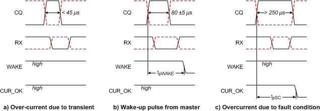 Figure 8. Over-current and Wake Conditions for EN = H, TX = H (full lines); and TX = L (red dotted lines)
9.3.2 Current Limit Indication – Short Circuit Current Detection
The internal current limit indicator is gated with the wake logic and thus becomes active only under certain conditions of the CQ-voltage (see Table 4).
9.3.3 Active Current Limit Condition: VTHL > VCQ ≥ VTHH
If the output current at CQ remains at the internally set current limit IO(LIM) for a duration longer than a wake-up pulse (longer than 80 μs), the CUR_OK pin is driven logic low, indicating an over-current condition. The CUR_OK pin returns to the high-impedance (inactive) state when the CQ pin is no longer in a current limit condition. The state diagram shown in Figure 9 illustrates the various states; and, under what conditions the device transitions from one state to another.
9.3.4 Inactive Current Limit Condition: VTHL < VCQ < VTHH
If the voltage at CQ is between the upper and lower receiver input threshold, CUR_OK remains high-impedance.
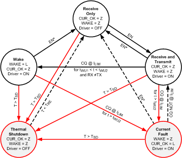 Figure 9. State Diagram of Device Transceiver
9.3.5 Over-temperature Detection
If the transceiver’s internal temperature exceeds its over-temperature threshold θTSD, the CQ driver and the voltage regulator (HVD101) are disabled. As soon as the temperature drops below the temperature threshold, the internal circuit re-enables the voltage regulator (HVD101) and the driver, subject to the state of the EN and TX pins.
9.3.6 CQ Current-limit Adjustment
The CQ driver current-limit is determined by the external resistor, RSET, at the ILIM_ADJ pin. Figure 2 shows the typical current-limit characteristics as a function of RSET.
9.3.7 Transceiver Function Tables
Table 1. Driver Function
| EN | TX | CQ | COMMENT |
|---|---|---|---|
| L or OPEN | X | Z | PHY is in ready-to-receive state |
| H | L | H | PHY CQ is sourcing current (high-side drive) |
| H | H or OPEN | L | PHY CQ is sinking current (low-side drive) |
Table 2. Receiver Function
| CQ Voltage | RX | COMMENT |
|---|---|---|
| VCQ < VCHL | H | Normal receive mode, input low |
| VTHL < VCQ < VTHH | ? | Indeterminate output, may be either High or Low |
| VTHH < VCQ | L | Normal receive mode, input high |
| OPEN | H | Failsafe output high |
Table 3. Wake-Up Function
| EN | TX | CQ VOLTAGE | WAKE | COMMENT |
|---|---|---|---|---|
| L | X | X | Z | PHY is in ready-to-receive state |
| H | H | VTHH < VCQ (tWU) | L | PHY receives High-level wake-up request from Master |
| H | X | VTHL < VCQ < VTHH | ? | Indeterminate output, may be either High or Low |
| H | L | VTHL > VCQ (tWU) | L | PHY receives Low-level wake-up request from Master |
Table 4. Current Limit Indicator Function (t > tWU)
| EN | TX | CQ VOLTAGE | CQ CURRENT | CUR_OK | COMMENT |
|---|---|---|---|---|---|
| H | H | VCQ ≥ VTHH | |ICQ| > IO(LIM) | L | CQ current is at the internal limit |
| |ICQ| < IO(LIM) | Z | Normal operation | |||
| VCQ < VTHH | X | Z | Current limit indicator is inactive | ||
| H | L | VCQ < VTHL | |ICQ| > IO(LIM) | L | CQ current is at the internal limit |
| |ICQ| < IO(LIM) | Z | Normal operation | |||
| VCQ ≥ VTHL | X | Z | Current limit indicator is inactive | ||
| L | X | X | X | Z | Driver is disabled, Current limit indicator is inactive |
Table 5. Temperature Indicator Function
| INTERNAL TEMPERATURE | OVER TEMPERATURE | TEMP_OK | COMMENT |
|---|---|---|---|
| T < TWARN | Not Over-Temperature | Z | Normal operation |
| TWARN < T↑ < TSD | Not Over-Temperature | L | Temperature warning |
| TSD < T | Over-Temperature Disabled | L | Over-Temperature disabled |
| TWARN < T↓ < TRE | Not Over-Temperature | L | Temperature recovery |
Table 6. Power Supply Indicator Function
| VL+ | VCC | PWR_OK | COMMENT |
|---|---|---|---|
| VL+ < VPG1 | VPOR2 < VCC < VPG2 | L | Both supplies too low |
| VPG1 < VL+ | VPOR2 < VCC < VPG2 | L | VCC too low |
| VL+ < VPG1 | VPG2 < VCC | L | VL+ too low |
| VPG1 < VL+ | VPG2 < VCC | Z | Both supplies correct |
9.3.8 Voltage Regulator (Not Available in SN65HVD102)
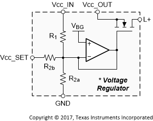
The SN65HVD101 integrates a linear voltage regulator which supplies power to external components as well as to the PHY itself. The voltage regulator is specified for L+ voltages in the range of 9V to 30V with respect to GND. The output voltage can be set using the Vcc_SET pin (see Figure 10). When this pin is left open (floating) then the output voltage is 5V. When it is connected to GND then the output voltage is 3.3V.
9.4 Device Functional Modes
The SN65HVD101 and SN65HVD102 can operate in three different modes:
- N-Switch SIO Mode
- P-Switch SIO Mode
- Push-Pull / Communication Mode
Set TX pin High and use EN pin as control for realizing the function of an N-switch (low-side driver) on CQ.
Set TX pin Low and use EN pin as control for realizing the function of a P-switch (high-side driver) on CQ.
Set EN pin high and toggle TX as control for realizing the function of a Push-Pull output on CQ.
Table 7 to Table 9 summarize the pin configurations to accomplish the above functional modes.
Table 7. N-Switch SIO Mode
| EN | TX | CQ |
|---|---|---|
| L | H | Hi-Z |
| H | H | N-Switch |
Table 8. P-Switch SIO Mode
| EN | TX | CQ |
|---|---|---|
| L | L | Hi-Z |
| H | L | P-Switch |
Table 9. Push-Pull / Communication Mode
| EN | TX | CQ |
|---|---|---|
| L | X | Hi-Z |
| H | H | N-Switch |
| H | L | P-Switch |