SLLSE84D May 2011 – May 2017 SN65HVD101 , SN65HVD102
PRODUCTION DATA.
- 1 Features
- 2 Applications
- 3 Description
- 4 Revision History
- 5 Device Comparison Table
- 6 Pin Configuration and Functions
- 7 Specifications
- 8 Parameter Measurement
-
9 Detailed Description
- 9.1 Overview
- 9.2 Functional Block Diagram
- 9.3
Feature Description
- 9.3.1 Wake-up Detection
- 9.3.2 Current Limit Indication - Short Circuit Current Detection
- 9.3.3 Active Current Limit Condition: VTHL > VCQ ≥ VTHH
- 9.3.4 Inactive Current Limit Condition: VTHL < VCQ < VTHH
- 9.3.5 Over-temperature Detection
- 9.3.6 CQ Current-limit Adjustment
- 9.3.7 Transceiver Function Tables
- 9.3.8 Voltage Regulator (Not Available in SN65HVD102)
- 9.4 Device Functional Modes
- 10Application and Implementation
- 11Power Supply Recommendations
- 12Layout
- 13Device and Documentation Support
- 14Mechanical, Packaging, and Orderable Information
Package Options
Mechanical Data (Package|Pins)
- RGB|20
Thermal pad, mechanical data (Package|Pins)
- RGB|20
Orderable Information
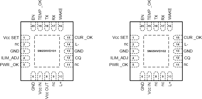
6 Pin Configuration and Functions
RGB Package
20-Pin QFN with Thermal Pad
Top View

Pin Functions
| PIN | DESCRIPTION | ||
|---|---|---|---|
| NAME | NUMBER | TYPE(1) | |
| IO-Link Interface | |||
| L+ | 10 | P | IO-Link supply voltage (24V nominal) |
| CQ | 12 | I/O | IO-Link data signal (bi-directional) |
| L– | 14 | P | IO-Link ground (connect to board ground) |
| Local Controller Interface | |||
| CUR_OK | 15 | OD | High-CQ-current fault indicator output signal from PHY to the microcontroller. Connect this pin via pull-up resistor to Vcc OUT. A LOW level indicates over-current condition. |
| WAKE | 16 | OD | Wake up indicator from the PHY to the local controller Connect this pin via pull-up resistor to Vcc OUT. |
| RX | 17 | O | PHY receive data output to the local controller |
| TX | 18 | I | PHY transmit data input from the local controller |
| EN | 20 | I | Driver enable input signal from the local controller |
| Power Supply Pins | |||
| VCC IN | 7 | A | Voltage supply input for SN65HVD102 Voltage sense feedback input for the voltage regulator of the SN65HVD101. Connect this pin to pin 8 either directly or through a current boost transistor. |
| VCC OUT | 8 | P | Not connected in SN65HVD102 Linear regulator output of SN65HVD101. Connect this pin to pin 7 either directly or through a current boost transistor. |
| GND | 3, 6, 13 | P | Logic ground potential |
| Special Connect Pins | |||
| VCC SET | 1 | I | Connect this pin to ground to make Vcc OUT = 3.3V. Leave this pin floating to make Vcc OUT = 5V. |
| ILIMADJ | 4 | A | Input for current limit adjustment. Connect resistor RSET between this pin and ground. For RSET values see Figure 2. |
| PWR_OK | 5 | OD | Power-Good indicator. Connect this pin via pull-up resistor to Vcc OUT. A HIGH at this pin indicates that L+ and Vcc OUT are at correct levels. |
| Temp_OK | 19 | OD | Temperature-Good indicator. Connect this pin via pull-up resistor to Vcc OUT. High-impedance at this pin indicates that the internal temperature is at a safe level. A low at this pin indicates the device is approaching thermal shutdown. |
| NC | 2, 9, 11 | – | No Connection. Leave these pins floating (open) |
(1) Type definitions: I = Input, I/O = Input/Output, A = Analog, O - CMOS Output, OD = Open Drain Output, P = Power