SLLS889C June 2008 – August 2016 SN65HVD1040A-Q1
PRODUCTION DATA.
- 1 Features
- 2 Applications
- 3 Description
- 4 Revision History
- 5 Description (continued)
- 6 Pin Configuration and Functions
- 7 Specifications
- 8 Parameter Measurement Information
- 9 Detailed Description
- 10Application and Implementation
- 11Power Supply Recommendations
- 12Layout
- 13Device and Documentation Support
- 14Mechanical, Packaging, and Orderable Information
Package Options
Mechanical Data (Package|Pins)
- D|8
Thermal pad, mechanical data (Package|Pins)
Orderable Information
9 Detailed Description
9.1 Overview
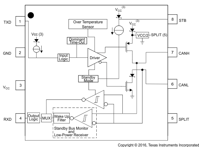
The SN65HVD1040A-Q1 CAN tranceiver is compatible with the ISO 11898-2 high-speed CAN (Controller Area Network) physical layer standard. The device is designed to interface between the differential bus lines in controller area network and the CAN protocol controller at data rates up to 1 Mbps.
9.2 Functional Block Diagram

9.3 Feature Description
9.3.1 Operating Modes
The device has two main operating modes: normal mode and standby mode. Operating mode selection is made through the STB input pin.
Table 2. Operating Modes
| STB PIN | MODE | DRIVER | RECEIVER | RXD PIN |
|---|---|---|---|---|
| LOW | NORMAL | Enabled (On) | Enabled (On) | Mirrors CAN bus |
| HIGH | STANDBY | Disabled (Off) | Low-power wake-up receiver and bus monitor enabled (On) | Low = wake-up request received High = no wake-up request received |
9.3.1.1 Bus States by Mode
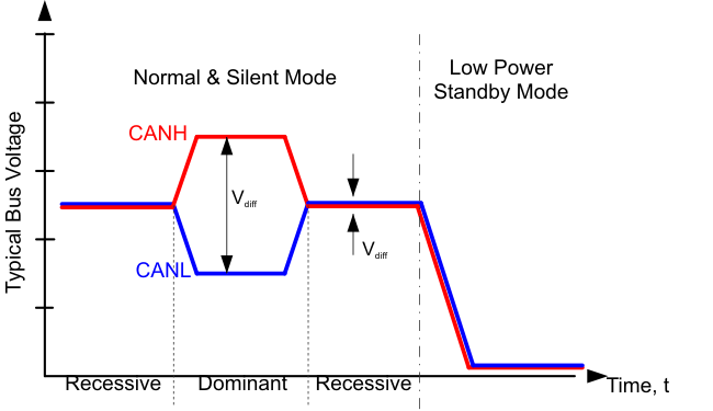
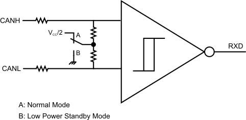
The CAN bus has three valid states during powered operation depending on the mode of the device. In normal mode the bus may be dominant (logic low) where the bus lines are driven differentially apart or recessive (logic high) where the bus lines are biased to VCC/2 through the high-ohmic internal input resistors RIN of the receiver. The third state is low-power standby mode where the bus lines are biased to GND through the high-ohmic internal input resistors RIN of the receiver.


9.3.1.2 Normal Mode
This is the normal operating mode of the device. It is selected by setting STB low. The CAN driver and receiver are fully operational and CAN communication is bidirectional. The driver is translating a digital input on TXD to a differential output on CANH and CANL. The receiver is translating the differential signal from CANH and CANL to a digital output on RXD. In recessive state the bus pins are biased to 0.5 × VCC. In dominant state the bus pins (CANH and CANL) are driven differentially apart. Logic high is equivalent to recessive on the bus and logic low is equivalent to a dominant (differential) signal on the bus.
The SPLIT pin is biased to 0.5 × VCC for bus common-mode bus voltage bias stabilization in split termination network applications (see Application and Implementation).
9.3.1.3 Standby Mode and RXD Wake-Up Request
This is the low-power mode of the device. It is selected by setting STB high. The CAN driver and main receiver are turned off and bidirectional CAN communication is not possible. The low-power receiver and bus monitor are enabled to allow for wake-up requests through the bus. A wake-up request will be output to RXD (driven low) for any dominant bus transmissions longer than the filter time tBUS. The local protocol controller (MCU) should monitor RXD for transitions and then reactivate the device to normal mode based on the wake-up request. The CAN bus pins are weakly pulled to GND and the SPLIT pin is off (floating).
 Figure 17. Standby Mode Low-Power Receiver and Bus Monitor Behavior
9.3.2 Protection Features
9.3.2.1 TXD Dominant State Time-Out
During normal mode (the only mode in which the CAN driver is active) the TXD dominant time-out circuit prevents the transceiver from blocking network communication in event of a hardware or software failure where TXD is held dominant longer than the time-out period tDST. The dominant time-out circuit is triggered by a falling edge on TXD. If no rising edge is seen before the time-out constant of the circuit expires (tDST), the CAN bus driver is disabled, thus freeing the bus for communication between other network nodes. The CAN driver is re-activated when a recessive signal is seen on the TXD pin, thus clearing the dominant state time-out. The CAN bus pins are biased to recessive level during a TXD dominant state time-out and SPLIT remains on.
NOTE
The maximum dominant TXD time allowed by the TXD Dominant state time-out limits the minimum possible data rate of the device. The CAN protocol allows a maximum of 11 successive dominant bits (on TXD) for the worst case, where 5 successive dominant bits are followed immediately by an error frame. This, along with the t(dom) minimum, limits the minimum bit rate. The minimum bit rate may be calculated by: Minimum Bit Rate = 11/t(dom)
9.3.2.2 Thermal Shutdown
If the junction temperature of the device exceeds the thermal shutdown threshold the device turns off the CAN driver circuits, including the SPLIT pin. This condition is cleared when the temperature drops below the thermal shutdown temperature of the device.
9.3.2.3 Undervoltage Lockout and Unpowered Device
The device has undervoltage detection and lockout on the VCC supply. If an undervoltage condition is detected on VCC, the device protects the bus.
The TXD pin is pulled up to VCC to force a recessive input level if the pin floats. The STB is pulled up to VCC to force the device in standby mode (low power) if the pin floats.
The bus pins (CANH, CANL, and SPLIT) all have extremely low leakage currents when the device is unpowered so it does not load down the bus but be an ideal passive load to the bus. This is critical, especially if some nodes of the network are unpowered while the rest of the network remains in operation.
9.4 Device Functional Modes
Table 3 and Table 4 lists the functions of this device.
Table 3. Driver Function Table(1)
| INPUTS | OUTPUTS | BUS STATE | ||
|---|---|---|---|---|
| TXD | STB | CANH | CANL | |
| L | L | H | L | Dominant |
| H | L | Z | Z | Recessive |
| Open | L | Z | Z | Recessive |
| X | H or Open | Y | Y | Recessive |
Table 4. Receiver Function Table
| DIFFERENTIAL INPUTS VID = V(CANH) – V(CANL) |
STB | OUTPUT RXD |
BUS STATE |
|---|---|---|---|
| VID ≥ 0.9 V | L | L | Dominant |
| VID ≥ 1.15 V | H or Open | L | Dominant |
| 0.5 V < VID < 0.9 V | X | ? | ? |
| VID ≤ 0.5 V | X | H | Recessive |
| Open | X | H | Recessive |
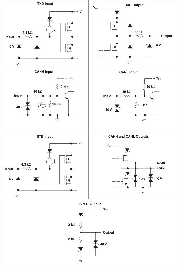
 Figure 18. Equivalent Input and Output Schematic Diagrams